Optical waveguide element

a technology of optical waveguides and elements, applied in non-linear optics, instruments, optics, etc., can solve the problems of affecting the operation point of a product, affecting the efficiency of the manufacturing process, so as to achieve efficient diffusion of charges generated in the substrate, efficiently dispersed, and efficient dispersion

Active Publication Date: 2015-03-19
SUMITOMO OSAKA CEMENT CO LTD
View PDF21 Cites 1 Cited by
  • Summary
  • Abstract
  • Description
  • Claims
  • Application Information

AI Technical Summary

Benefits of technology

The present invention relates to an improved electronic device (ECD) component used in lightwave communication systems called Optically Wave Guide Elements (OWG). These components include various layers like dielectric films, metal plugs, and insulating materials. By creating these layers within specific regions where they interact well together, efficient charging/discharges may occur without causing problems such as increased power consumption due to reduced current flow caused by impurities from outside sources. This results in longer life span and less heat dissipation during operation compared to previous designs. Additionally, this design allows for effective application of AC bias fields while minimizing unwanted signals. Overall, this technology improves efficiency and reliability in Lightwaves Communications

Problems solved by technology

The technical problem addressed in this patented text relates to prevention of unwanted electrical effects from affects when light travels along certain paths due to variations in temperatures during use. This can cause issues like signal loss or distortions over time if there are no effective ways for these modifications.

Method used


Image

  • Optical waveguide element
  • Optical waveguide element
  • Optical waveguide element

Examples


Embodiment Construction

[0034]Hereinafter, an optical waveguide element of the present invention will be described in detail.

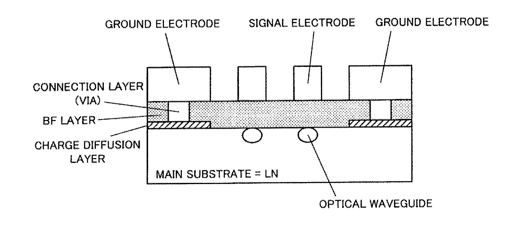
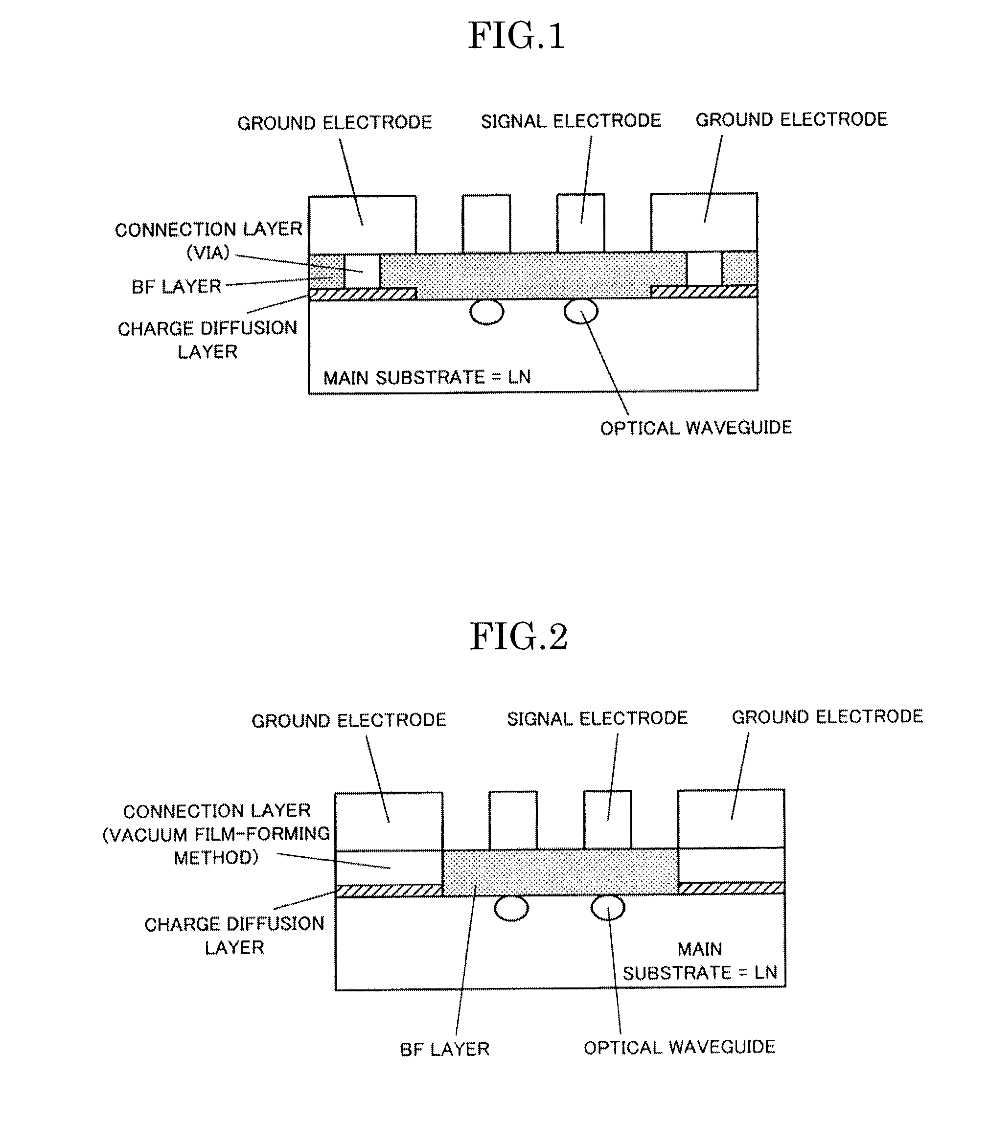
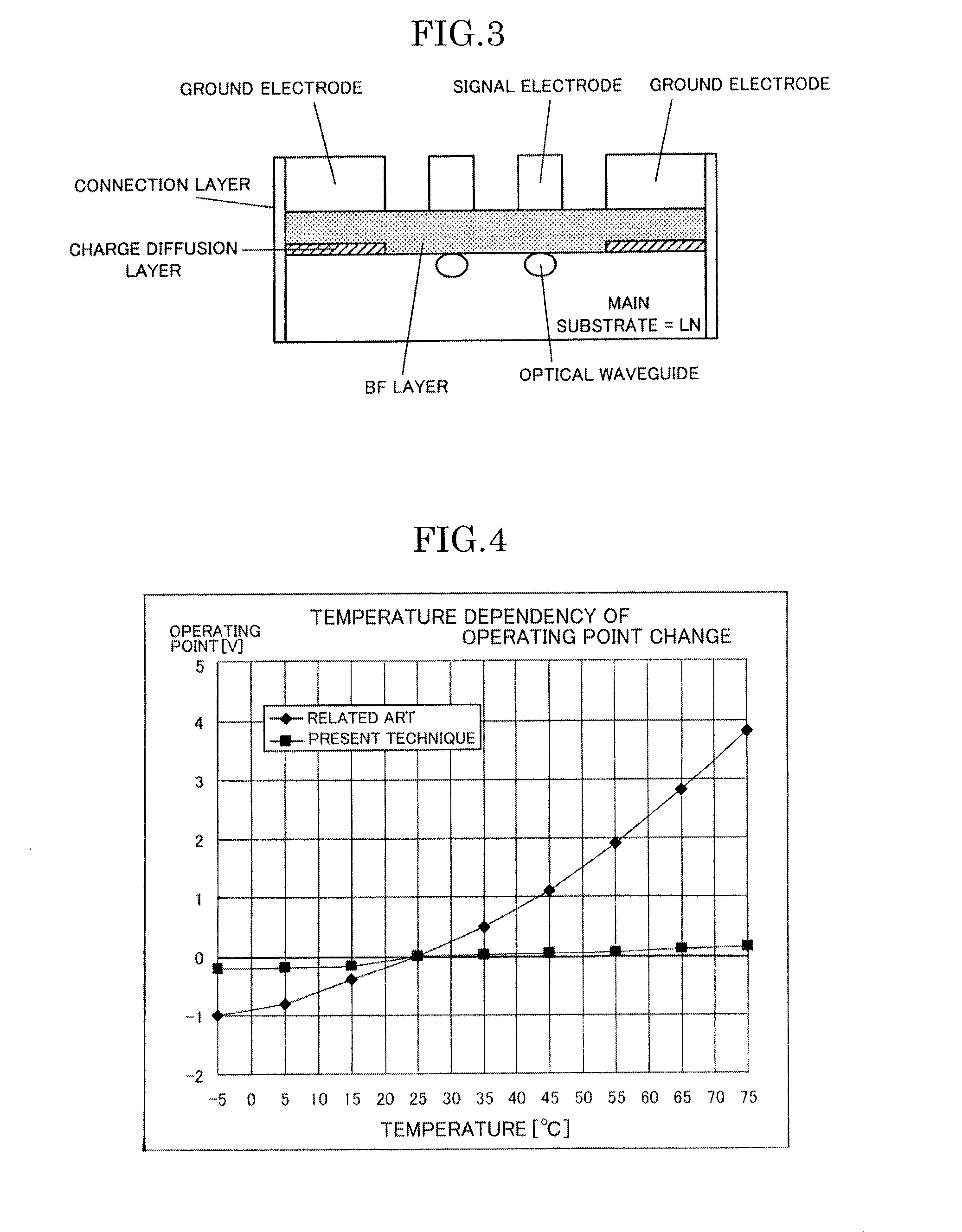
[0035]As illustrated in FIG. 1, the optical waveguide element of the present invention is an optical waveguide element including a substrate having an electro-optical effect, optical waveguides formed in the substrate, a buffer layer (BF layer) formed on the substrate, and modulation electrodes (signal electrode and ground electrode) that are formed on the buffer layer and modulate optical waves propagating through the optical waveguides, in which a charge diffusion layer that diffuses charges generated in the substrate is formed between the substrate and the buffer layer, and the charge diffusion layer is electrically connected with a ground electrode constituting the modulation electrode.

[0036]As the substrate used in the present invention, a substrate for which a material having an electro-optical effect can be used, and, for example, a substrate made of lithium niobate, lithium tant


PUM


Abstract

An object of the present invention is to provide an optical waveguide element that effectively diffuses charges accumulated in a substrate, and suppress DC drift or temperature drift. The optical waveguide element includes a substrate having an electro-optical effect, optical waveguides formed in the substrate, a buffer layer (BF layer) formed on the substrate, and modulation electrodes (signal electrode and ground electrode) that are formed on the buffer layer and modulate optical waves propagating through the optical waveguides, a charge diffusion layer that diffuses charges generated in the substrate is formed between the substrate and the buffer layer, and the charge diffusion layer is electrically connected with a ground electrode constituting the modulation electrode.

Description


Claims


Application Information

Patent Timeline
Owner SUMITOMO OSAKA CEMENT CO LTD
Why Eureka
Try Eureka