Display device
a technology of display device and display screen, which is applied in the field of display device, can solve the problems of high black luminance, high luminance of display screen, and high luminance of known display device, and achieve the effect of improving the utilization efficiency of ligh
- Summary
- Abstract
- Description
- Claims
- Application Information
AI Technical Summary
Benefits of technology
Problems solved by technology
Method used
Image

Examples
first embodiment
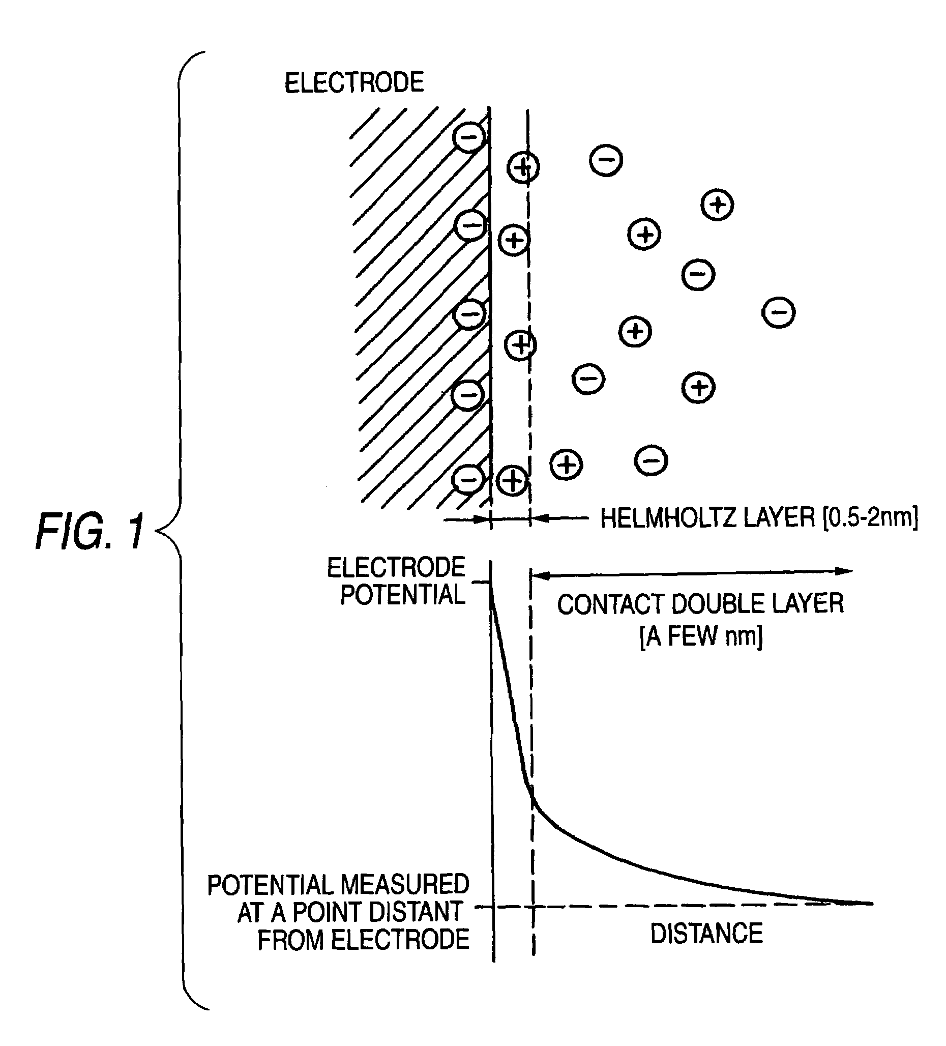
[0071]First, an electrowetting phenomenon utilized by the invention will be briefly described by reference to FIGS. 1 and 2.
[0072]When an electrode is dipped into an electrolyte (solution), an interface is formed along a contact surface existing between the surface of the electrode and the solution. As shown in FIG. 1, a so-called electrical double layer EDL is formed on the interface from metal ions and free electrons of the electrode and electrolyte ions of the solution. When an electric field is applied to the metal-electrolyte interface, a change in surface tension is induced. This phenomenon is called the electrowetting phenomenon.
[0073]Any conductive material may be used as the electrode. For instance, the electrode may be made of metal such as Pt, Au, Ni, or Al; a metallic oxide such as SnO2, In2O3, RuO2, or TiO2; a semiconductor such as Ge, Si, or GaAs; or a carbon-based conductive material such as graphite, glassy carbon, or diamond.
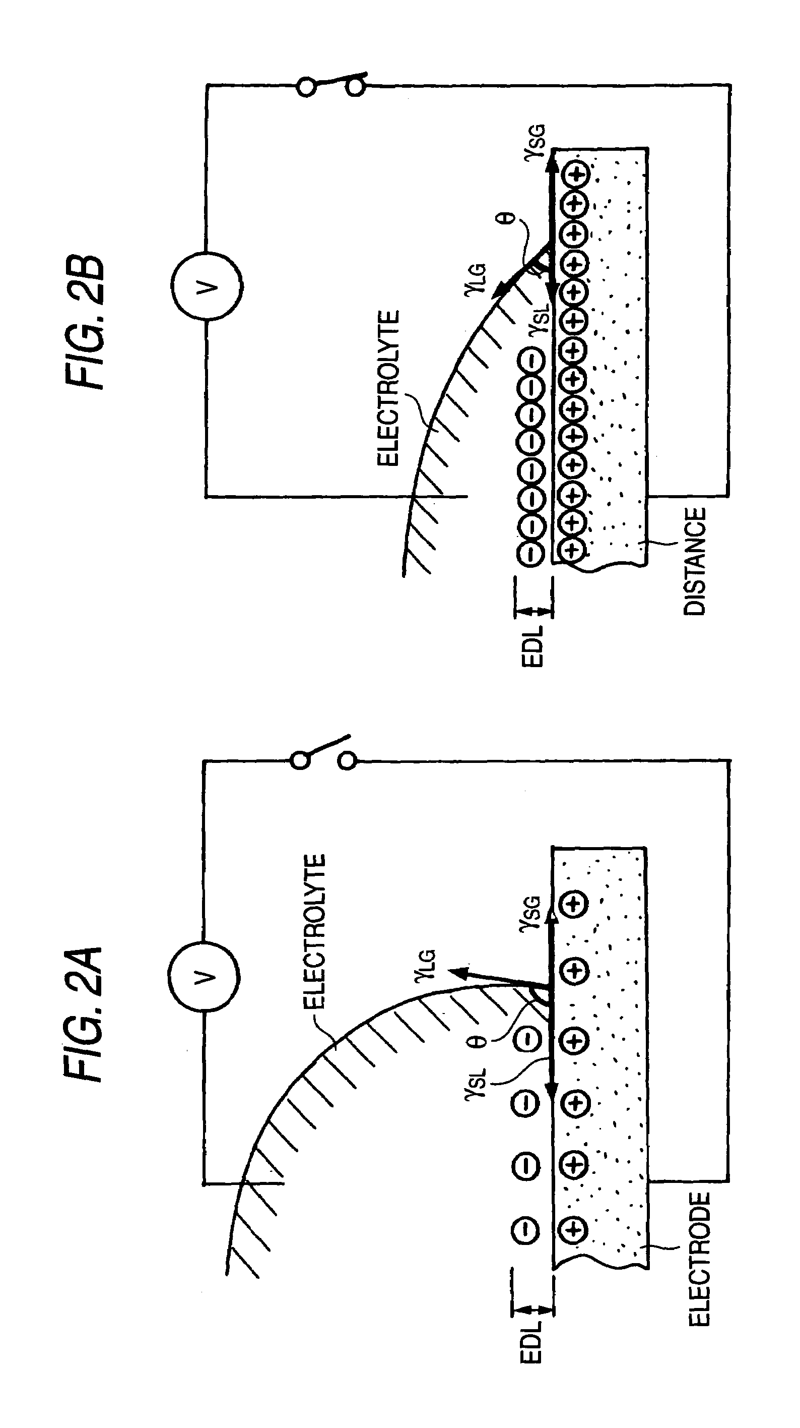
[0074]FIG. 2 is a view for describing a chan
second embodiment
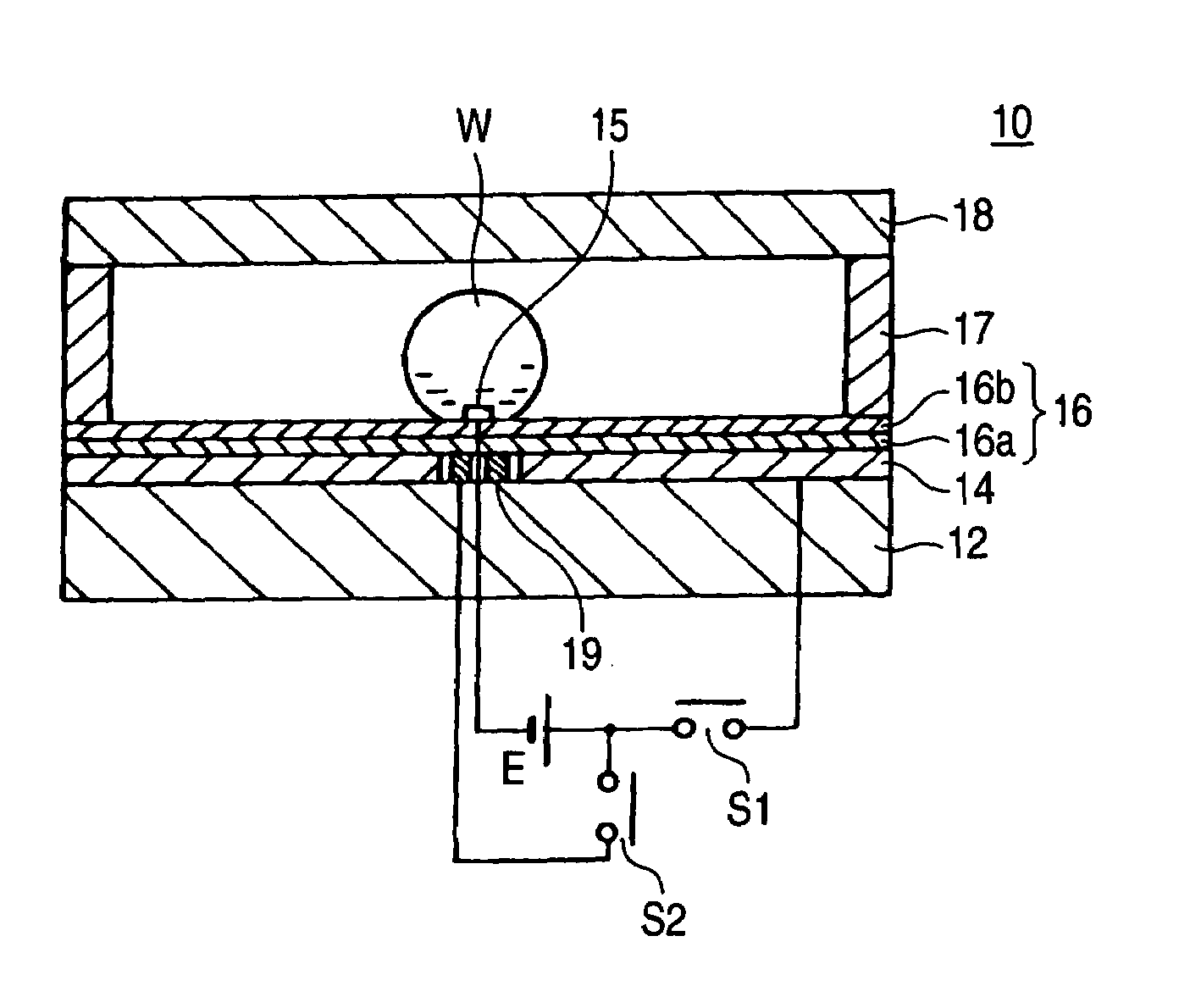
[0118]FIG. 7 relates to a second embodiment of the invention, wherein FIG. 7A is a longitudinal cross-sectional view taken at the time of dark display and FIG. 7B is a longitudinal cross-sectional view taken at the time of bright display.
[0119]In the drawing, reference numeral 20 designates a display device according to the second embodiment of the invention; the display device is identical in configuration with the display device of the first embodiment, and hence its explanation is omitted.
[0120]A difference between the display devices of the first and second embodiments lies in that a third switch S3 is provided and the first transparent electrode is actively utilized even at the time of restoration of a droplet, to thereby accelerate a shift from the dark display to the bright display to a much greater extent.
[0121]The switch S3 that operates in the same manner as does the switch S2 (i.e., the switch is activated when the switch S1 is in an OFF position and is deactivated when the
third embodiment
[0127]FIG. 8 relates to a modification of the location where the third transparent electrode of the third embodiment of the invention is mounted. FIG. 8A shows an example in which the third transparent electrode is provided at the center of the cavity's ceiling; FIG. 8B shows an example in which the third transparent electrode is provided in an annular pattern on the cavity's ceiling; and FIG. 8C shows an example in which the third transparent electrode is provided in a cavity partition.
[0128]FIGS. 8A to 8C are views showing that rapid conversion arises from the dark display to the bright display. The display device is entirely identical in configuration with that shown in FIG. 3, except the position where the third transparent electrode 19 is provided, and hence description of the configuration and operation of the display device will be omitted.
[0129]FIG. 8A will first be described.
[0130]In FIG. 8A, the third transparent electrode 19 is a circular transparent electrode having a small
PUM
 Abstract
Description
Claims
Application Information
 - R&D Engineer
- R&D Manager
- IP Professional
- Industry Leading Data Capabilities
- Powerful AI technology
- Patent DNA Extraction
Browse by: Latest US Patents, China's latest patents, Technical Efficacy Thesaurus, Application Domain, Technology Topic.
© 2024 PatSnap. All rights reserved.Legal|Privacy policy|Modern Slavery Act Transparency Statement|Sitemap