Method for manufacturing solar battery

A technology of solar cells and manufacturing methods, applied in the direction of final product manufacturing, sustainable manufacturing/processing, circuits, etc., can solve problems affecting the quality of silicon wafers, high cost of photomask manufacturing process, and complicated steps, etc., to improve photoelectric conversion efficiency Effect

Inactive Publication Date: 2010-01-13
KUNSHAN ZHONGCHEN SILICON CO LTD
View PDF0 Cites 5 Cited by
  • Summary
  • Abstract
  • Description
  • Claims
  • Application Information

AI Technical Summary

Problems solved by technology

[0004] In general, the manufacturing method of the backside contact cell uses the lithography etching process of opening the photomask multiple times on the bottom surface of the silicon wafer, and the p + type (boron), n + The pattern (phosphorus) area and the electrode are scre

Method used


Image

  • Method for manufacturing solar battery
  • Method for manufacturing solar battery
  • Method for manufacturing solar battery

Examples


Example Embodiment

[0023] The characteristics of the present invention can be clearly understood by referring to the detailed description of the drawings and embodiments of the present case.

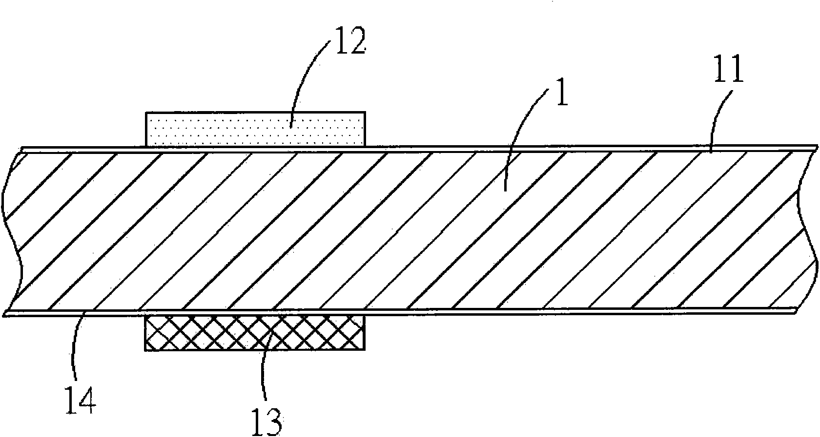
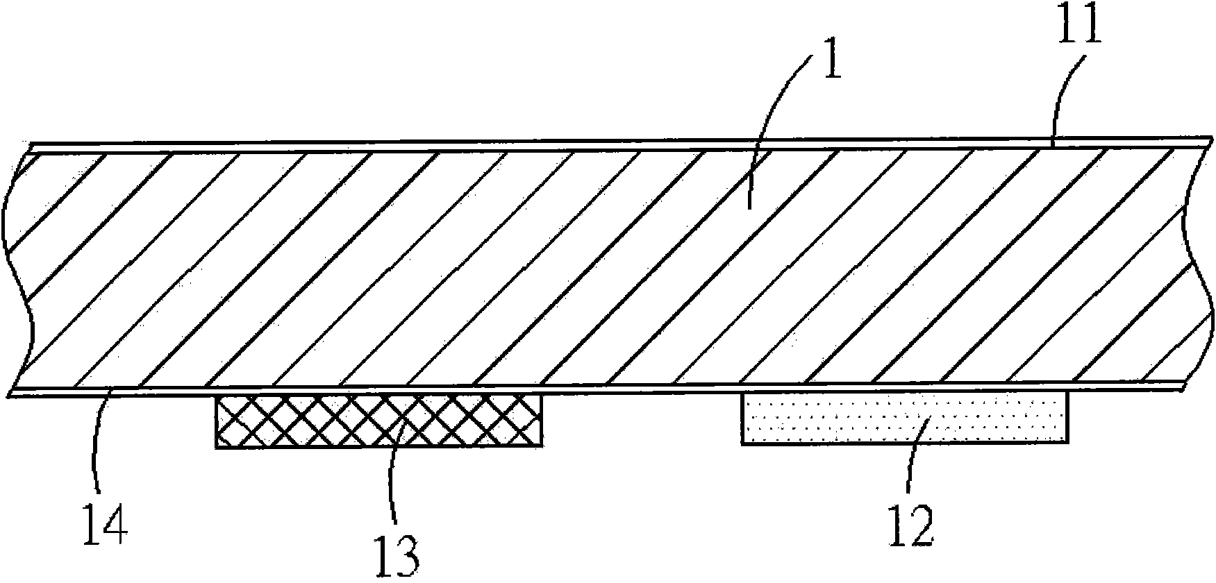
[0024] The manufacturing method of the solar cell of the present invention includes at least the following steps:

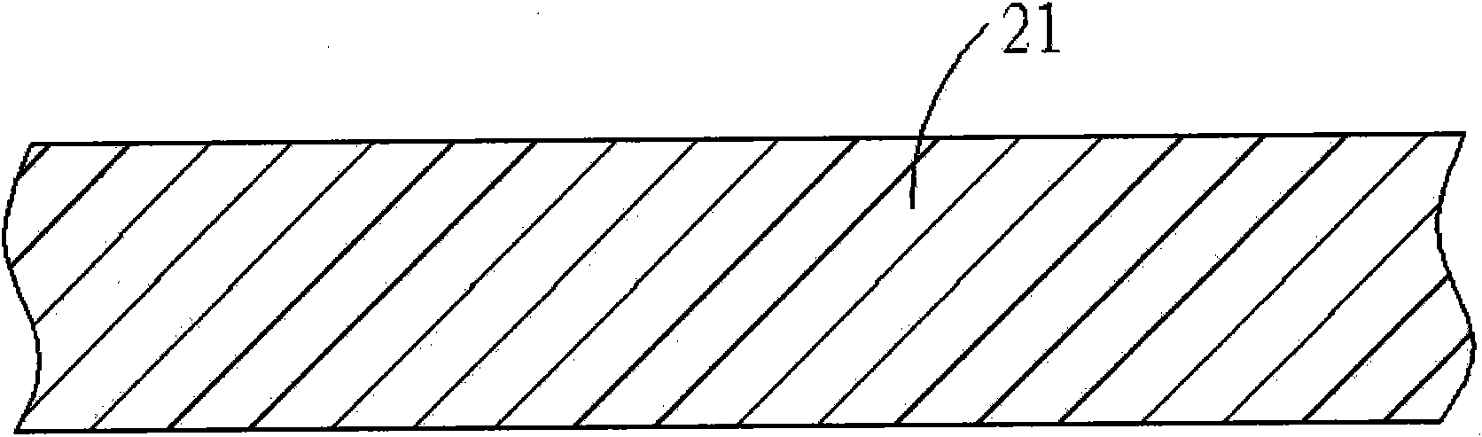
[0025] Step A, provide a wafer 21, such as image 3 As shown, the wafer 21 may be an n-type monocrystalline silicon wafer;

[0026] Step C1: First and second passivation layers 22 and 23 are provided, and first and second passivation layers 22 and 23 are respectively provided on the bottom and top surfaces of wafer 21, such as Figure 4A As shown, the first and second passivation layers 22, 23 can be ultra-thin, with a thickness of about 20-50 The first passivation layer 22 can be made of amorphous silicon or silicon with dopants such as carbon, nitrogen and oxygen deposited on the bottom surface of the wafer 21, and the second passivation layer 23 can be made of silicon oxide or doped non-crystalline


PUM


Abstract

The invention relates to a method for manufacturing a solar battery. Two electrode layers of the solar battery are arranged on the same side of a wafer so that the sunlight incoming from the other side cannot be shielded by the electrode layers to promote the photoelectric conversion efficiency; besides, each electrode layer uses a shielding layer to perform vapor deposition process molding without the processes of lithography and etching of any photomask and surely without a high-temperature process which destroys the quality of the wafer.

Description


Claims


Application Information

Patent Timeline
Owner KUNSHAN ZHONGCHEN SILICON CO LTD
Why Eureka
Try Eureka