Light-emitting diode packaging structure
A light-emitting diode and packaging structure technology, which is applied in the direction of electrical components, circuits, semiconductor devices, etc., can solve the problems of light scattering, light loss, direct contact between light-emitting diode grains and fluorescent colloid layers, etc., to ensure the service life , reduce heat energy, increase the overall light output effect
- Summary
- Abstract
- Description
- Claims
- Application Information
AI Technical Summary
Benefits of technology
Problems solved by technology
Method used
Image

Examples
Embodiment Construction
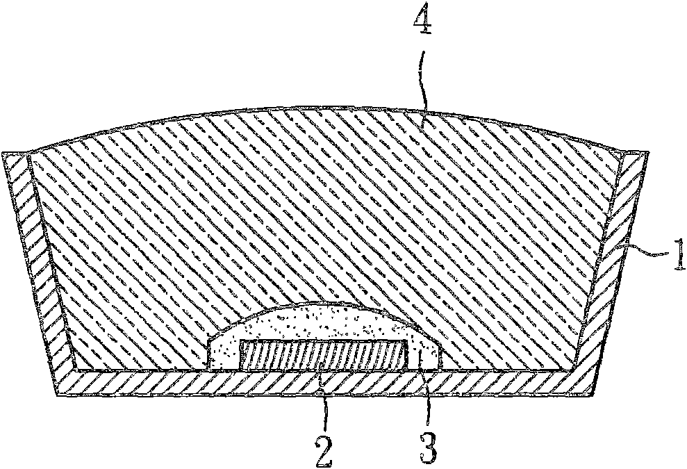
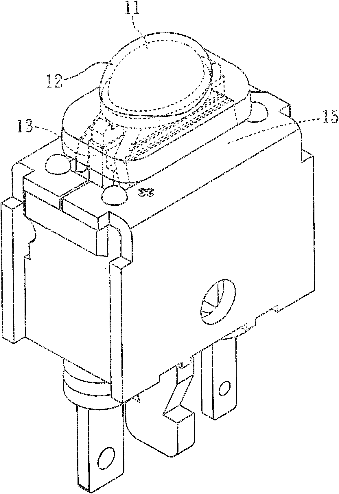
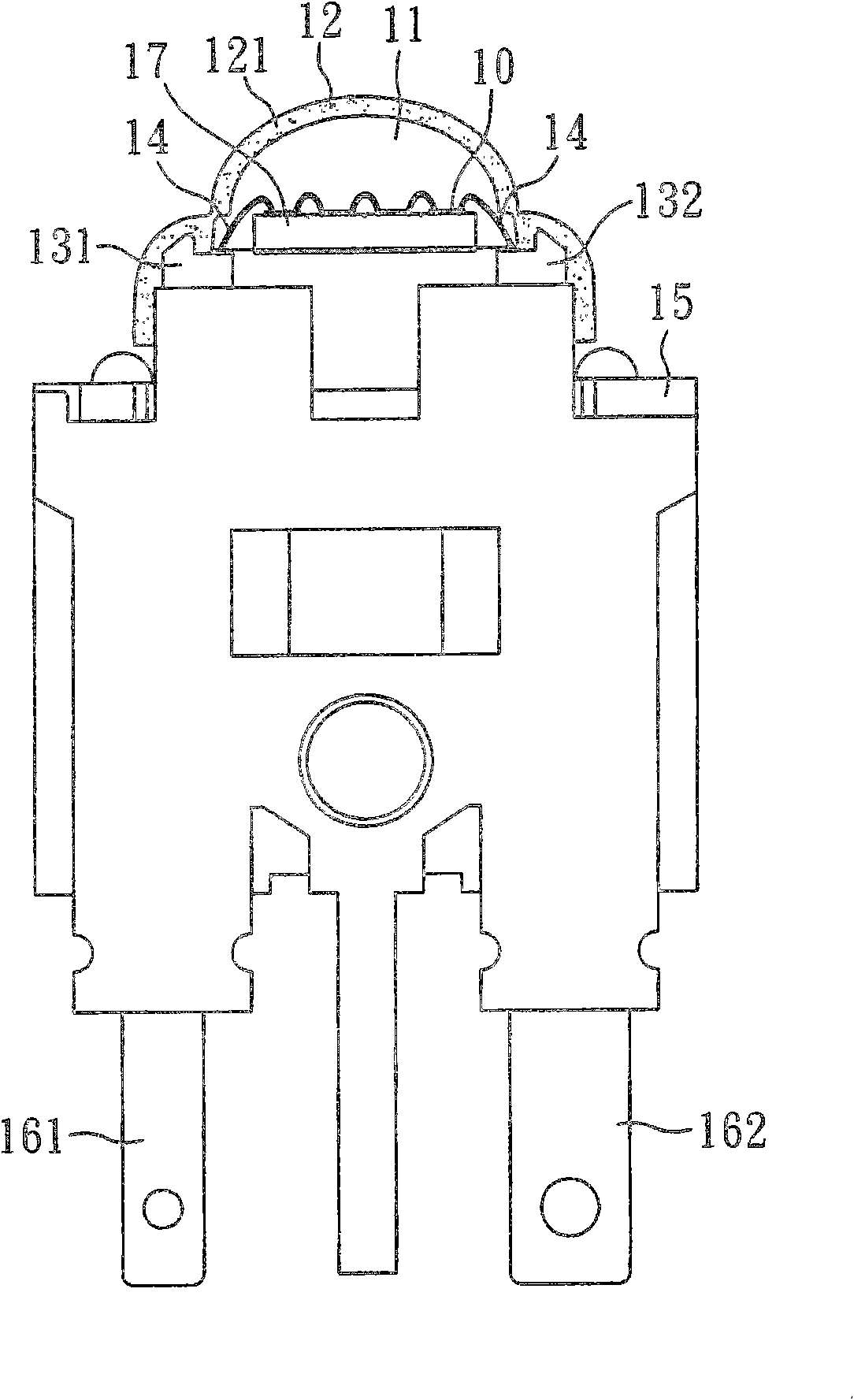
[0018] refer to figure 2 and image 3 , are respectively a perspective view and a cross-sectional view of a light emitting diode packaging structure in a preferred embodiment of the present invention. The LED packaging structure includes a light emitting diode crystal grain 10 , a transparent colloidal layer 11 , a fluorescent colloidal layer 12 , a conductive seat 13 , and a heat dissipation shell 15 . The LED crystal grain 10 used in this embodiment is a blue light crystal grain, and an ultraviolet light diode crystal grain can also be used, which is located on the die-bonding plane 17, and the LED crystal grain 10 is electrically connected to the conductive seat 13 through two wires 14 to conduct electricity. The seat 13 is composed of a positive pole bracket 131 and a negative pole bracket 132 representing two different polarities. It can be seen from the figure that the two brackets extend to the ends to form two external electrical pins 161 and 162 . The conductive base
PUM
 Abstract
Description
Claims
Application Information
 - R&D Engineer
- R&D Manager
- IP Professional
- Industry Leading Data Capabilities
- Powerful AI technology
- Patent DNA Extraction
Browse by: Latest US Patents, China's latest patents, Technical Efficacy Thesaurus, Application Domain, Technology Topic.
© 2024 PatSnap. All rights reserved.Legal|Privacy policy|Modern Slavery Act Transparency Statement|Sitemap