Semiconductor element, packaging structure and forming method of semiconductor element

A semiconductor and component technology, applied in the field of bump structure technology, can solve the problem of high risk of short circuit and achieve the effect of avoiding short circuit or bridging

Active Publication Date: 2011-08-10
TAIWAN SEMICON MFG CO LTD
View PDF5 Cites 5 Cited by
  • Summary
  • Abstract
  • Description
  • Claims
  • Application Information

AI Technical Summary

Problems solved by technology

However, the quality and reliability of lead-free solder bumps do not always meet the requirements
For smaller pitches and hi

Method used


Image

  • Semiconductor element, packaging structure and forming method of semiconductor element
  • Semiconductor element, packaging structure and forming method of semiconductor element
  • Semiconductor element, packaging structure and forming method of semiconductor element

Examples


Embodiment Construction

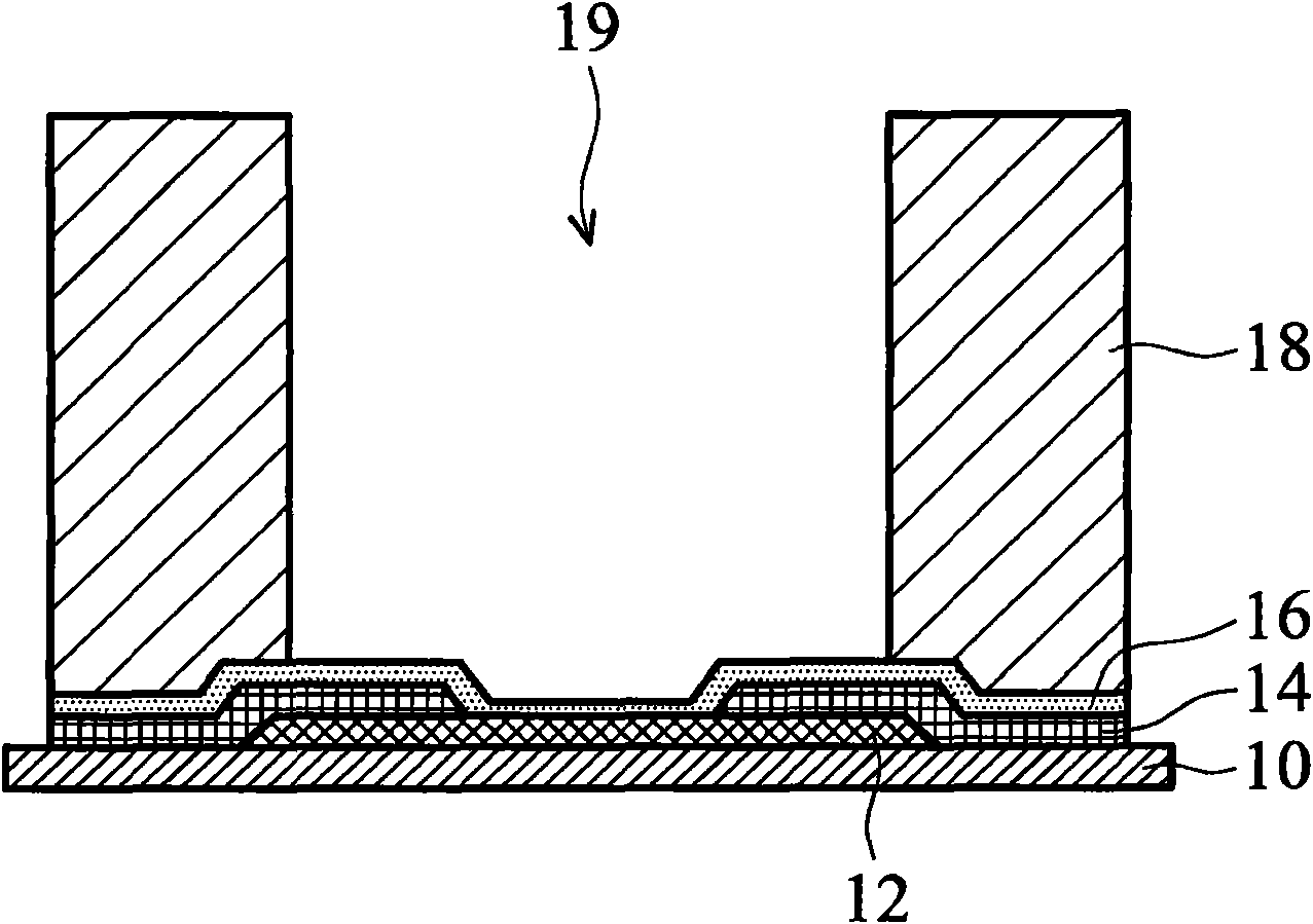
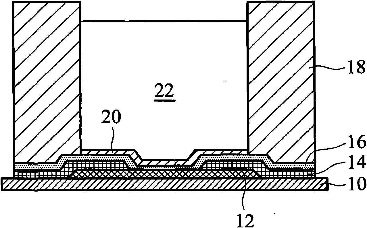
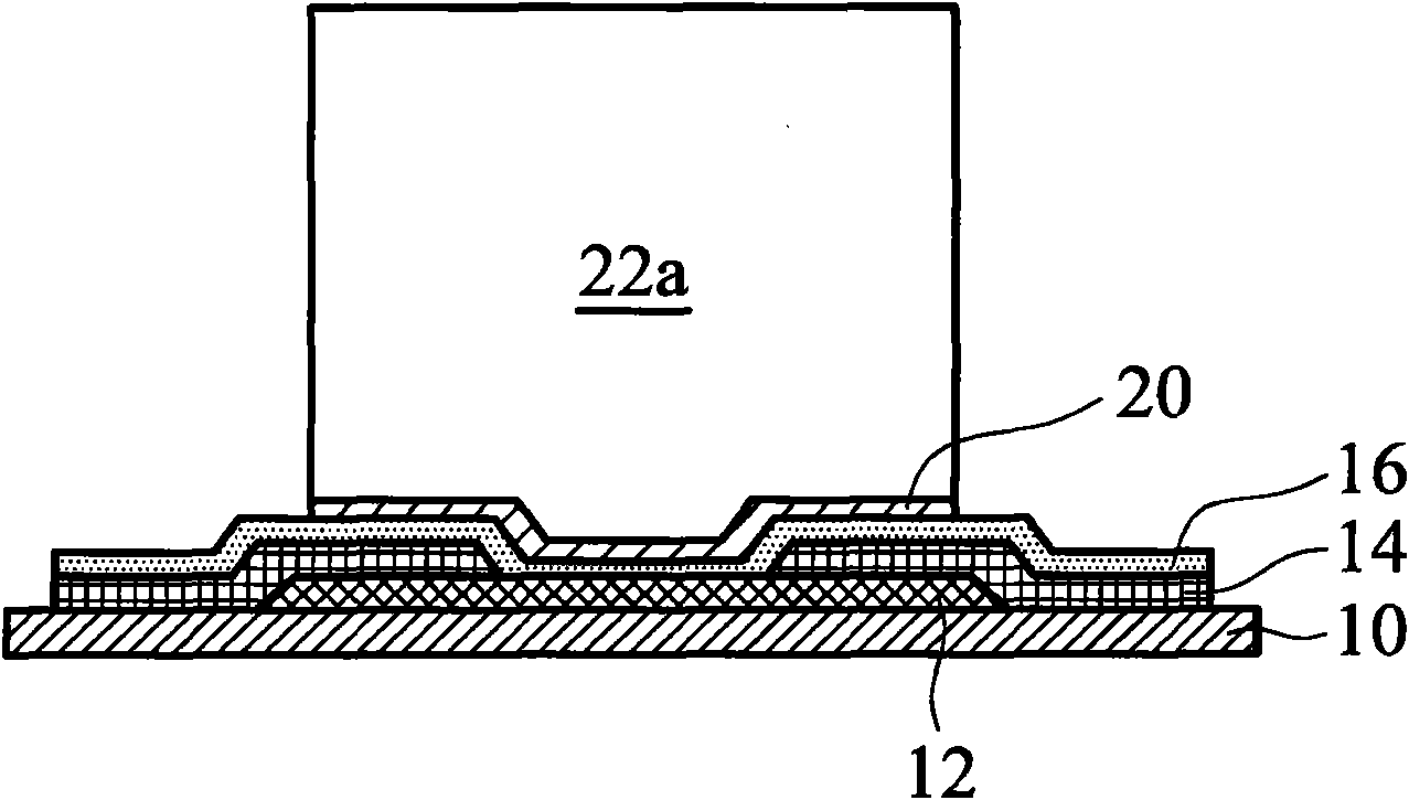
[0014] The bumping process in semiconductor devices described below can be applied to flip-chip packaging, wafer-level chip-scale packaging (WLCSP), three-dimensional integrated circuit (3D-IC) stacking, and / or any advanced packaging technologies. Embodiments relate to solder bumps for semiconductor devices and methods of forming the same. In the following description, various specific examples will be preceded to facilitate those skilled in the art to have a comprehensive understanding of the present invention. However, those skilled in the art should understand that the actual operation does not need to fully comply with these special cases. In some instances, structures and processes well known in the art have not been described in detail to avoid unnecessarily obscuring the disclosure. In the following description, "an embodiment" refers to a particular feature, structure, or structure in which at least one embodiment is combined. Thus, references to "an embodiment" in di


PUM


Abstract

The invention provides a semiconductor element, a packaging structure and a forming method of a semiconductor element. A solder bump provided in the semiconductor element is disposed on a welding pad and is electrically connected to the welding pad. A metal cover layer is disposed at a part of the welding bump. The melting point of the metal cover layer is higher than that of the welding bump. The invention is advantageous in that the metal cover layer can be used as a hardstop element; the bump structure after packaging can maintain a consistent height; the problem of short circuit or bridgejoint can be reduced and even prevented.

Description


Claims


Application Information

Patent Timeline
Owner TAIWAN SEMICON MFG CO LTD
Why Eureka
Try Eureka