Cutting machine for cutting silicon chips

A technology of cutting machine and silicon wafer, applied in the field of cutting machine and silicon wafer cutting machine, can solve the problems such as the weak connection between the silicon wafer and the pallet, affecting the yield of the silicon wafer, and the falling damage of the silicon wafer, so as to achieve a simple structure, Improve yield and avoid drop damage

Inactive Publication Date: 2012-02-29
ZHENJIANG GANGNAN ELECTRIC
View PDF4 Cites 0 Cited by
  • Summary
  • Abstract
  • Description
  • Claims
  • Application Information

AI Technical Summary

Benefits of technology

This technology improves upon existing methods by creating an anti-drop fence around each piece of crystal material used for manufacturing electronic devices such as solar cells or integrated circuits (ICs). By adding this roller design on both surfaces, there are fewer points where they come into direct physical contact that could cause harm during handling processes like transportation. Additionally, it simplifies the process of connecting two materials together while also ensuring better stability over time. Overall, these technical improvements improve productivity and quality control across various industries including semiconductor industry production.

Problems solved by technology

This patented technical problem addressed by the present inventors relating to improving the stability and reliability of conventional methods that use hardened steel wiring or other materials like sandwiches on top of the surface being processed (silicone) when driving small tools through these surfaces.

Method used


Image

  • Cutting machine for cutting silicon chips
  • Cutting machine for cutting silicon chips

Examples


Embodiment Construction

[0008] The present invention will be further described below in conjunction with accompanying drawing.

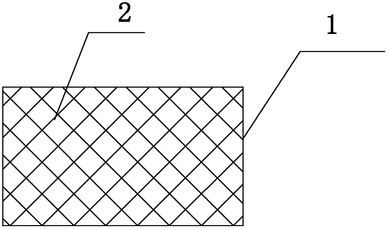
[0009] As shown in the figure, in order to solve the above technical problems, a cutting machine for cutting silicon wafers according to the present invention includes a supporting plate 1, a glass plate 2, the supporting plate 1 and the glass plate 2 are connected into one body, and the supporting plate 1 is used to To connect the silicon chip, the surface of the supporting plate 1 in contact with the silicon chip is provided with a knurling pattern 2. Since the surface of the supporting plate in contact with the silicon chip is provided with a knurling pattern, the friction between the supporting plate and the silicon chip is improved. force, so that the connection between the silicon wafer and the supporting plate is more firm, and the silicon wafer is prevented from falling and damaged, thereby improving the yield of the silicon wafer; in addition, the present invention has


PUM


Abstract

The invention provides a cutting machine for cutting silicon chips, which comprises a support plate and a glass plate, wherein knurling patterns are arranged on the side of the support plate in contact with the silicon chips. Because the knurling patterns are arranged on the side of the support plate in contact with the silicon chips, the contact friction force of the support plate and the silicon chips is improved, the connection between the silicon chips and the support plate is firmer, the damage to the silicon chips caused by falling is avoided, and the finished product rate of the silicon chips is improved. In addition, the cutting machine has a simple structure.

Description


Claims


Application Information

Patent Timeline
Owner ZHENJIANG GANGNAN ELECTRIC
Why Eureka
Try Eureka