LED vertical chip structure and manufacturing method

A technology of chip structure and manufacturing method, applied in electrical components, circuits, semiconductor devices, etc., can solve the problems of low yield and complex LED chip manufacturing process, and achieve the effects of high yield, uniform current distribution, and large light-emitting area

Inactive Publication Date: 2013-08-21
XI AN JIAOTONG UNIV
View PDF6 Cites 13 Cited by
  • Summary
  • Abstract
  • Description
  • Claims
  • Application Information

AI Technical Summary

Benefits of technology

In this new design for an improved type of semiconductor device called silicone lamps or microLEDs (μLED). These devices use special materials that have better electrical properties than regular sapphires due to their lower melting point temperature. However, they also require more energy input from external sources like electricity because it requires them to generate enough heat to operate properly. To solve these issues, there are some technical means described below.

Problems solved by technology

This patented technical solution described for making high brightness blue laser diodes (BLD) involves combining different materials together through various methods like chemical vapor deposition (CVD), metal organic chemical vapour phase synthesis (MOVPE). These techniques help improve efficiency, lifespan, speed up reaction time, reduce resistance between components, enhance cooling capabilities, and create smaller devices that require fewer electrical connections than previous designs. However, these new technologies also lead to issues related to device failure caused by excessively large electric currents flowing along their leads during operation.

Method used


Image

  • LED vertical chip structure and manufacturing method
  • LED vertical chip structure and manufacturing method

Examples


Embodiment Construction

[0020] The present invention is described in further detail below in conjunction with accompanying drawing:

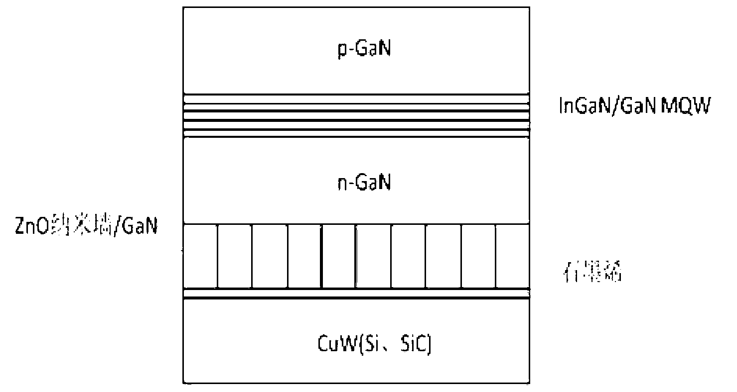
[0021] refer to figure 1 , LED vertical chip structure described in the present invention is provided with substrate, graphene layer, ZnO nano wall / GaN, n-GaN layer, InGaN / GaN multiple quantum well and p-GaN successively from bottom to top, and described substrate is One of Si, SiC, CuW and Mo, the thickness of the substrate is 20-500 μm, the thickness of the graphene layer is 1-10 layers of graphene, and the thickness of the ZnO nanowall / GaN layer is 2-500 μm. 5 μm.

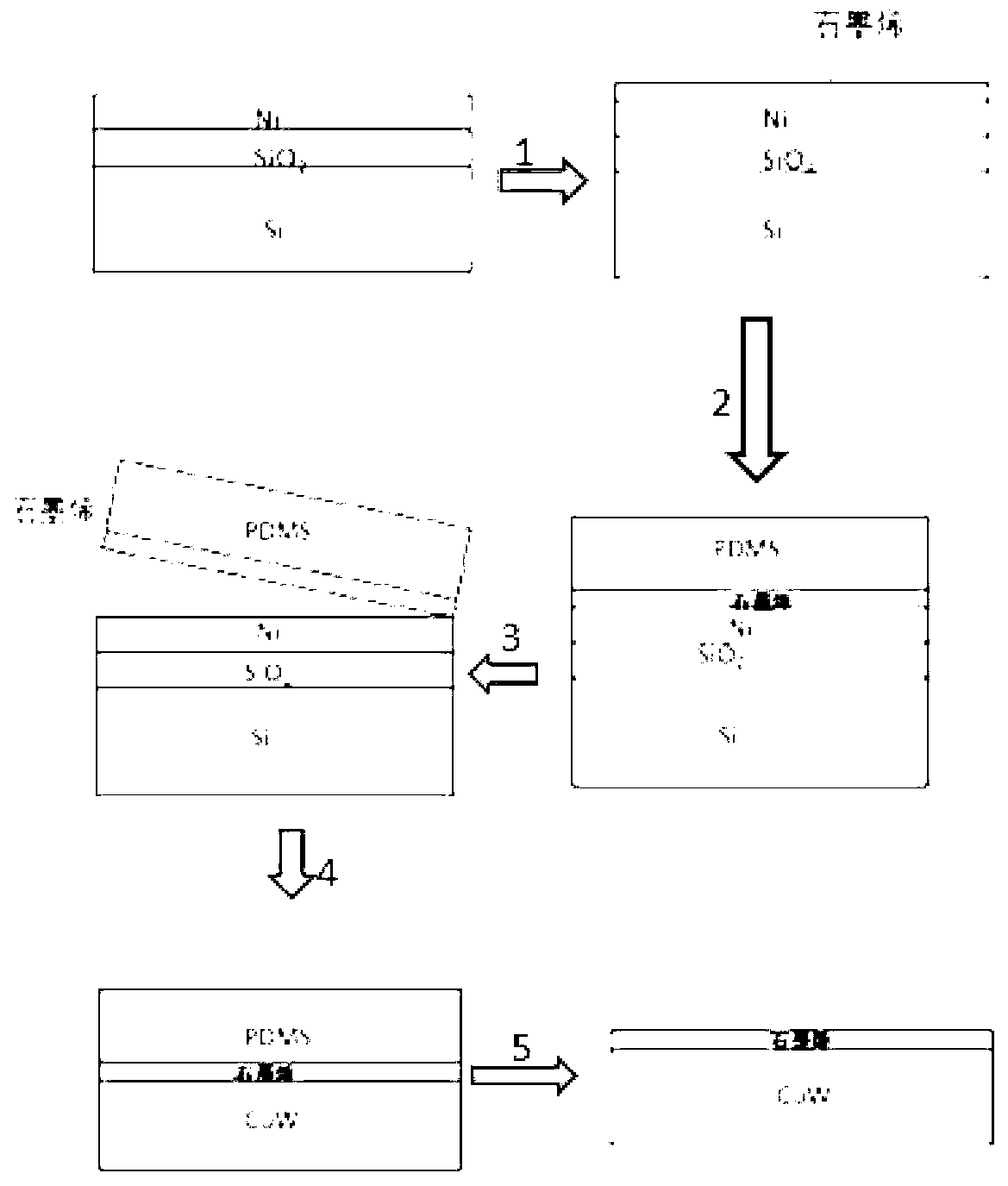
[0022] Correspondingly, refer to figure 2 , LED vertical chip manufacturing method of the present invention, comprises the following steps:

[0023] 1) On a silicon substrate, SiO with a thickness of 300nm is formed by diffusion furnace oxidation 2 , and then electron beam evaporation on SiO 2 Ni-coated silicon substrate with a thickness of 300nm can be obtained on the layer;

[0024] 2) Put th


PUM

PropertyMeasurementUnit
Thicknessaaaaaaaaaa
Thicknessaaaaaaaaaa

Abstract

The invention discloses an LED vertical chip structure and a manufacturing method. The LED vertical chip structure sequentially comprises a substrate, a graphene layer, a ZnO nanometer wall/ GaN, an n-GaN layer, an InGaN/ GaN multiple quantum well and a p-GaN from bottom to top. Compared with a traditional sapphire substrate LED chip, the LED vertical chip structure is large in lighting area and strong in heat dissipation capacity and has no current blocking effect. Meanwhile, due to the fact that the LED vertical chip directly extends outwards and grows, compared with a vertical structure LED prepared through a peeling-bonding technology, the LED vertical structure has the advantages that the processes of peeling and bonding are removed, the processes are simplified, and yield is high.

Description


Claims


Application Information

Patent Timeline
Owner XI AN JIAOTONG UNIV
Why Eureka
Try Eureka