Image sensor module with reduced overall thickness
An image sensing and image sensing element technology, applied in the field of image sensing modules, can solve the problems of reducing the overall thickness, the overall thickness cannot be effectively reduced, etc., and achieve the effect of reducing the overall thickness
- Summary
- Abstract
- Description
- Claims
- Application Information
AI Technical Summary
Problems solved by technology
Method used
Image

Examples
Example Embodiment
[0051] Example one
[0052] See Figure 2A to Figure 2D As shown, Figure 2A Is the top view of the flexible substrate before being bent, Figure 2B for Figure 2A 2B-2B cross-sectional schematic diagram, Figure 2C Is a schematic side view of the flexible substrate before being bent, Figure 2D It is a schematic side view of the flexible substrate after being bent. As can be seen from the above figures, the first embodiment of the present invention provides an image sensor module Z with reduced overall thickness, which includes: a substrate unit 1, a transparent unit 2, an image sensor unit 3 and a lens unit 4.
[0053] First, cooperate Figure 2A versus Figure 2B As shown, the substrate unit 1 includes at least one flexible substrate 10, wherein the flexible substrate 10 has at least one through opening 100. The light transmitting unit 2 includes at least one light transmitting element 20 disposed on the upper surface of the flexible substrate 10 and corresponding to the through o
Example Embodiment
[0057] Example two
[0058] See image 3 As shown, the second embodiment of the present invention provides an image sensing module Z with reduced overall thickness, which includes: a substrate unit 1, a light transmitting unit (not shown), an image sensing unit (not shown), and A lens unit 4. by image 3 versus Figure 2A The comparison shows that the biggest difference between the second embodiment of the present invention and the first embodiment is that: in the second embodiment, the substrate unit 1 includes a plurality of electronic components 11 arranged on a flexible substrate 10, and the above-mentioned plurality of electronic components 11 Two of them can be electrically connected to each other through a first conductive circuit W1 disposed on the main body portion 10A and one of the extension portions 10B "simultaneously". In other words, any two of the plurality of electronic components 11 of the present invention can selectively pass through (1) "One and only the first
Example Embodiment
[0059] Example three
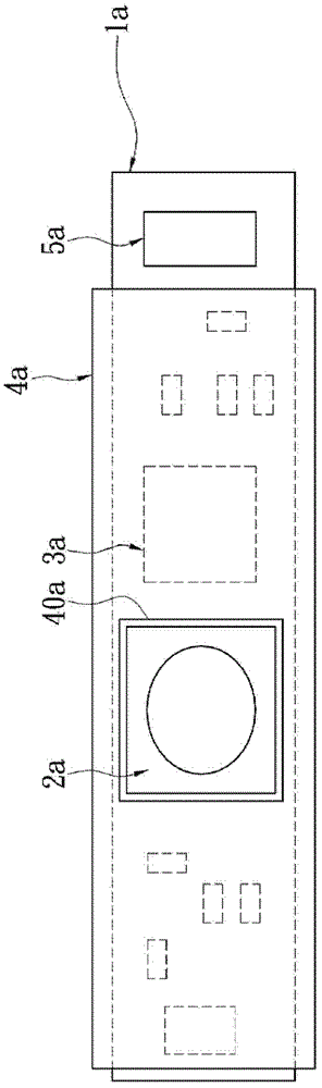
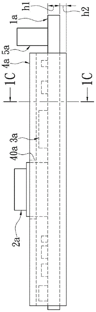
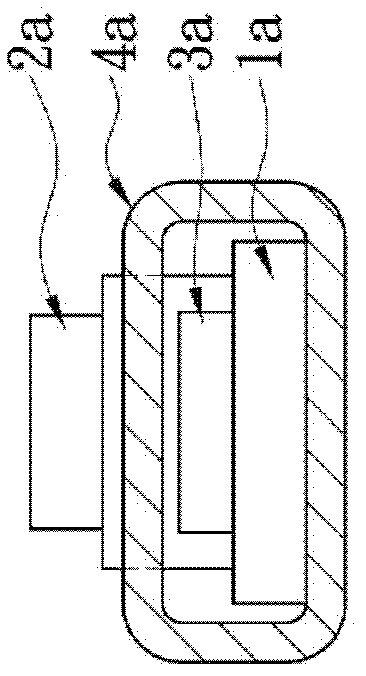
[0060] See Figure 4 As shown, the third embodiment of the present invention provides an image sensor module Z with a reduced overall thickness, which includes: a substrate unit 1, a light-transmitting unit 2, an image sensor unit 3, and a lens unit 4. The substrate unit 1 includes at least one flexible substrate 10, wherein the flexible substrate 10 has at least one through opening 100. The light transmitting unit 2 includes at least one light transmitting element 20 disposed on the upper surface of the flexible substrate 10 and corresponding to the through opening 100. The image sensing unit 3 includes at least one image sensing element 30 disposed on the lower surface of the light-transmitting element 20 and embedded in the through opening 100, wherein the image sensing element 30 is electrically connected to the flexible substrate 10. The lens unit 4 includes an opaque frame 40 disposed on the upper surface of the flexible substrate 10 and surrounding the
PUM
 Abstract
Description
Claims
Application Information
 - R&D Engineer
- R&D Manager
- IP Professional
- Industry Leading Data Capabilities
- Powerful AI technology
- Patent DNA Extraction
Browse by: Latest US Patents, China's latest patents, Technical Efficacy Thesaurus, Application Domain, Technology Topic.
© 2024 PatSnap. All rights reserved.Legal|Privacy policy|Modern Slavery Act Transparency Statement|Sitemap