OLED array substrate, manufacturing method thereof, displaying panel and displaying device

A technology for array substrates and display panels, which is applied in semiconductor/solid-state device manufacturing, semiconductor devices, electrical components, etc., can solve the problems of two-layer ITO film layers that are prone to mildew and high cost of reflective layers, and achieve a small overall thickness, Reduce the effect of mildew

Active Publication Date: 2014-07-09
WUHAN TIANMA MICRO ELECTRONICS CO LTD +1
View PDF5 Cites 1 Cited by
  • Summary
  • Abstract
  • Description
  • Claims
  • Application Information

AI Technical Summary

Problems solved by technology

[0004] The embodiment of the present invention provides an OLED array substrate and its preparation method, a display panel and a display device, which are used to improve the problems in the prior art that the cost of the reflective layer is high and the two ITO film layers are prone to mildew

Method used


Image

  • OLED array substrate, manufacturing method thereof, displaying panel and displaying device
  • OLED array substrate, manufacturing method thereof, displaying panel and displaying device
  • OLED array substrate, manufacturing method thereof, displaying panel and displaying device

Examples


Example Embodiment

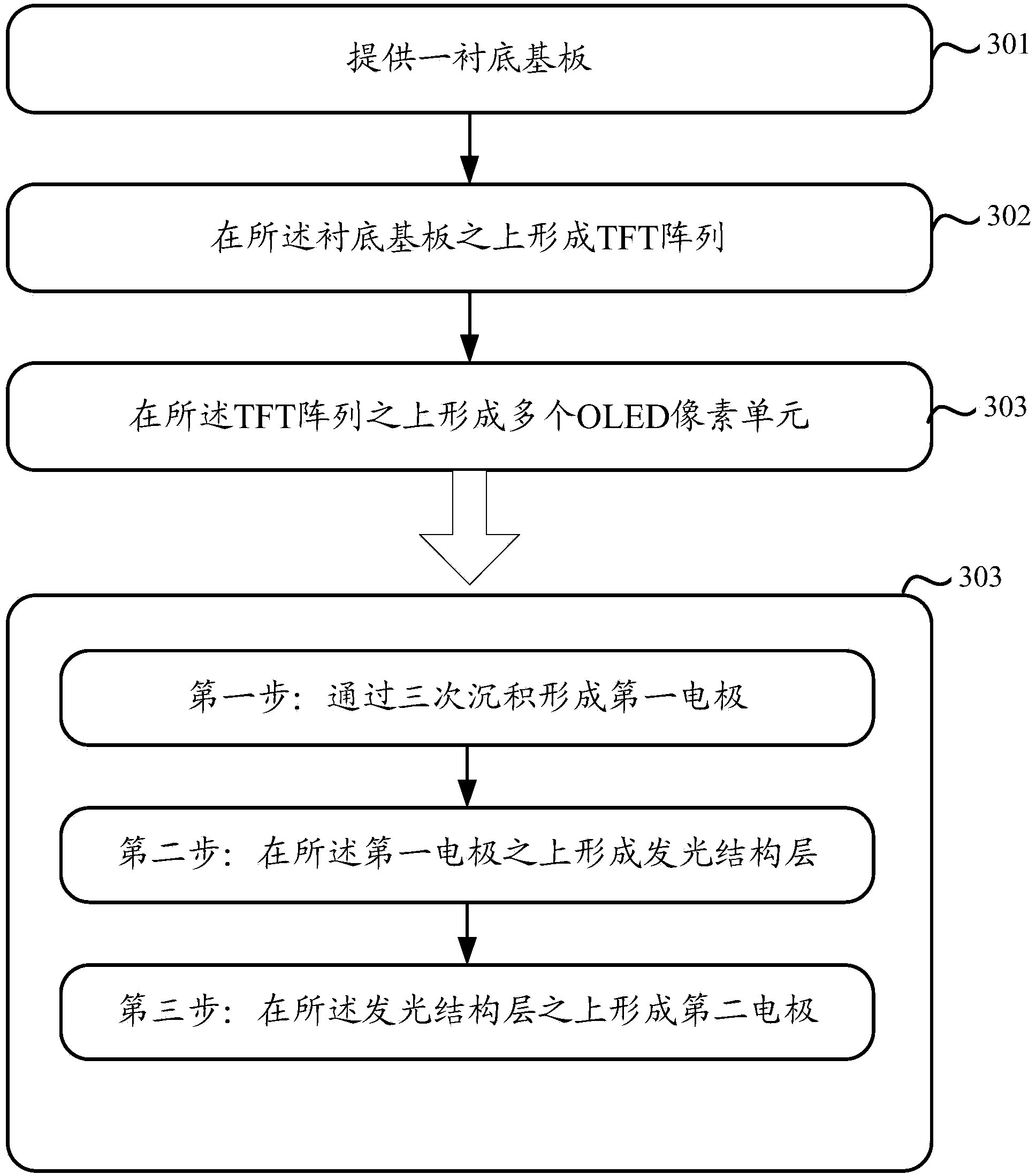
[0017] In order to make the objectives, technical solutions and advantages of the present invention clearer, the present invention will be further described in detail below in conjunction with the accompanying drawings. Obviously, the described embodiments are only a part of the embodiments of the present invention, rather than all of them. Based on the embodiments of the present invention, all other embodiments obtained by those of ordinary skill in the art without creative work shall fall within the protection scope of the present invention.

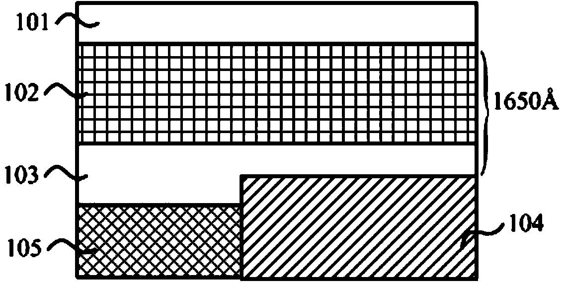
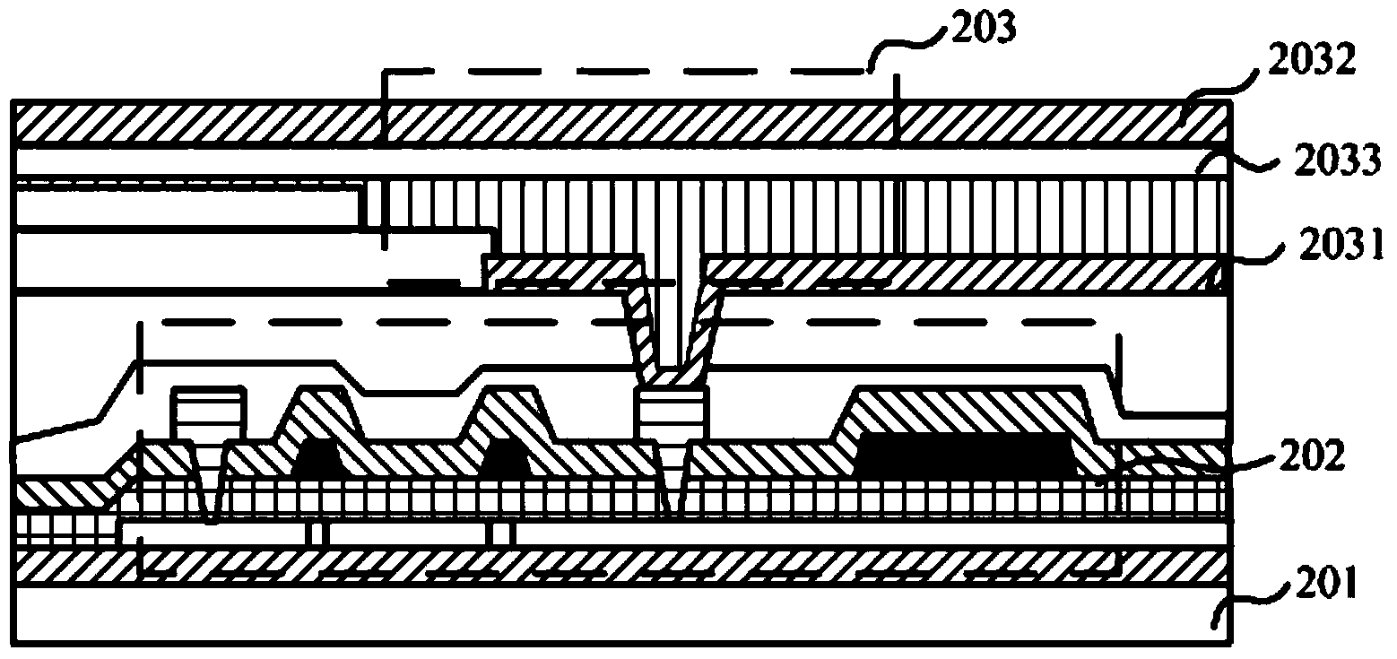
[0018] In the existing OLED display technology field, it can be divided into two types: bottom emission and top emission according to the direction of the emitted light. The schemes involved in the embodiments of the present invention are all top-emitting structures, and the top-emitting structure must meet the following requirements: the first electrode uses a conductive material with high reflectivity, the second electrode uses a conductive


PUM


Abstract

The invention discloses an OLED array substrate, a manufacturing method thereof, a displaying panel and a displaying device. The OLED array substrate comprises a plurality of OLED pixel units. Any OLED pixel unit comprises a first electrode, a second electrode and a light-emitting structure layer placed between the first electrode and the second electrode. Each first electrode comprises a metal single substance film layer placed on a bottom layer, an alloy film layer placed on the metal single substance film layer and an ITO film layer arranged on the alloy film layer. Each alloy film layer is a film layer formed by alloy formed by metal simple substance and mercury according to a set weight ratio. Accordingly, silver sulfide generation is avoided, good reflectivity and electric conductivity are guaranteed, and the phenomena of ITO mildewing of a whole reflecting layer are reduced.

Description


Claims


Application Information

Patent Timeline
Owner WUHAN TIANMA MICRO ELECTRONICS CO LTD
Why Eureka
Try Eureka