Viewing method for substrate with uneven surface

A technology for leveling the surface and substrate, applied in the field of inspection, can solve the problems that the carrier film cannot be seen through, increase the risk of damage, time-consuming and labor-intensive, etc., and achieve the effect of increasing the risk of chip damage, increasing production efficiency, and reducing the inspection process

Inactive Publication Date: 2014-07-23
YOMORE TECH
View PDF4 Cites 3 Cited by
  • Summary
  • Abstract
  • Description
  • Claims
  • Application Information

AI Technical Summary

Benefits of technology

The technical effect of this new technology allows for better quality control during semiconductor device fabrication by detecting defects on wafers before dicing them into separate chips or packaging it separately instead of relying solely upon visual detection alone. This results in improved productivity while reducing cost-effectiveness through reduced labor requirements and prevention of damaged devices caused by pulling away individual dies afterwards without requiring extra steps like cutting off any unwanted parts.

Problems solved by technology

This patented technical problem addressed by this patents relates to improving the efficiency at detecting defective wafers after they are mounted onto carrier films used in producing electronic devices such as IC's. Current methods require separate steps before pulling them away from the nonuniform surfaces formed on both sides of these substrate layers. These techniques increase costs associated with maintenance work while reducing productivity due to increased downtime caused by removing unnecessary components.

Method used


Image

  • Viewing method for substrate with uneven surface
  • Viewing method for substrate with uneven surface
  • Viewing method for substrate with uneven surface

Examples


Embodiment Construction

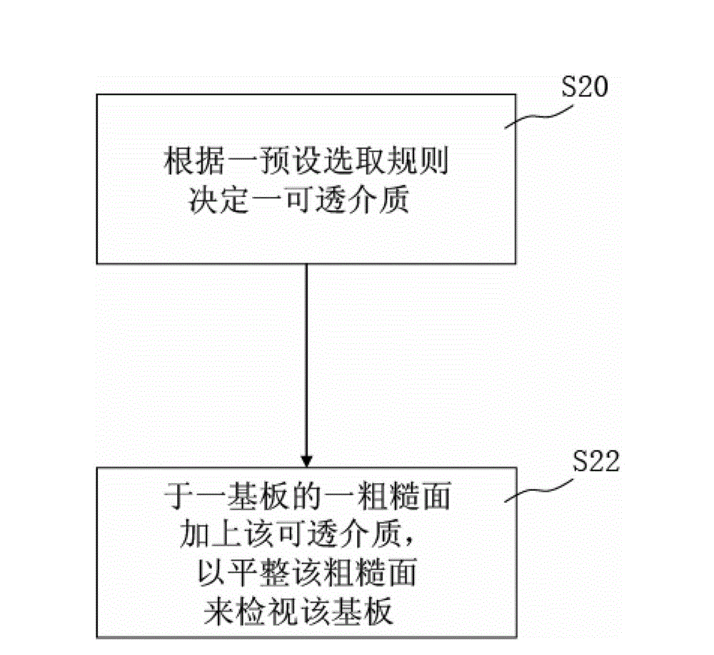
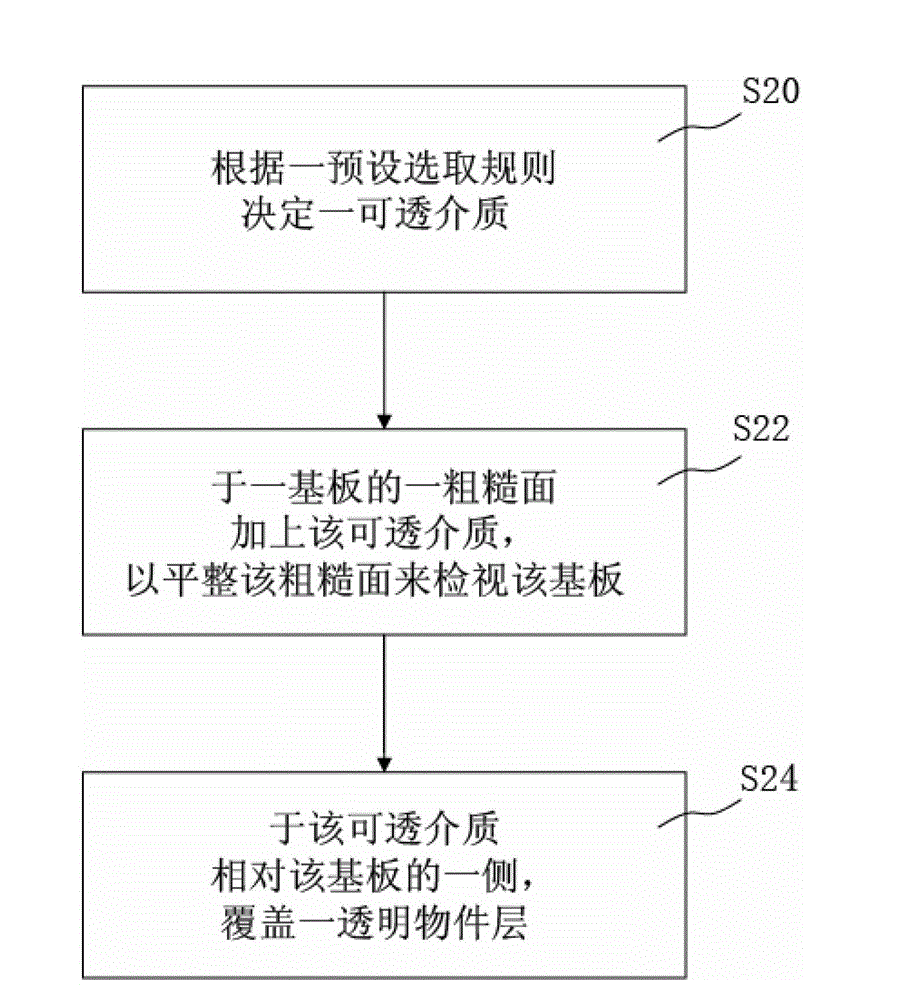
[0035] Please refer to Figure 2A as shown, Figure 2A It is a flowchart of an embodiment of the inspecting method for a substrate with an uneven surface of the present invention. In one embodiment, a method for inspecting a substrate with an uneven surface includes the following steps:

[0036] S20 determining a permeable medium according to a preset selection rule; and

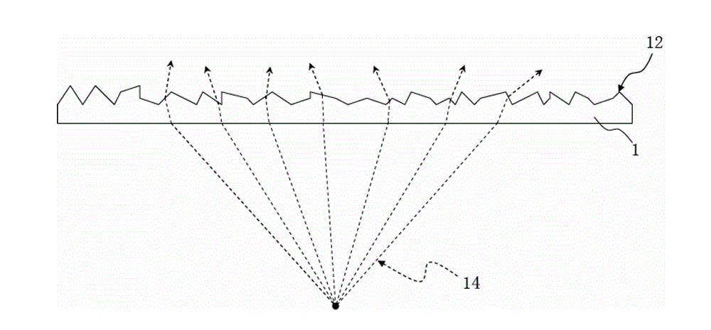
[0037] S22 adding the transparent medium on a rough surface of a substrate to flatten the rough surface to inspect the substrate.

[0038] Wherein, the selection rule is set by calculating a refractive index difference between the transparent medium and the substrate, and the smaller the refractive index difference is, the better the transparency is. For example, when the refractive index of the substrate is n 1 , the refractive index of the transparent medium is n 2 , then the calculation method of the refractive index difference value can be:

[0039]

[0040] According to the summary of the inventor


PUM


Abstract

The invention discloses a viewing method for a substrate with an uneven surface. The method comprises a step of setting a transparent medium according to preset selection principal, a step of adding the transparent medium on the rough surface of the substrate, and a step of viewing the substrate through smoothing the rough surface. The viewing method can be applied to wafer viewing, and an integrated circuit on a wafer can be viewed through the rough surface of a carrier film adhered to the wafer, thereby reducing a risk of destroying wafers and improving the yield of chip production.

Description


Claims


Application Information

Patent Timeline
Owner YOMORE TECH
Why Eureka
Try Eureka