Advanced back side process fabrication method for improving IGBT performance

A technology of backside technology and manufacturing method, which is applied in semiconductor/solid-state device manufacturing, electrical components, circuits, etc., and can solve the problem that the concentration and depth of the N-type buffer layer are difficult to meet the requirements, the activation efficiency is not high, and the improvement of device performance is small, etc. problem, to achieve performance optimization, reduce power consumption, and reduce the size of the device

Active Publication Date: 2015-06-17
SHANGHAI HUAHONG GRACE SEMICON MFG CORP
View PDF5 Cites 1 Cited by
  • Summary
  • Abstract
  • Description
  • Claims
  • Application Information

AI Technical Summary

Benefits of technology

This technology improves how much energy goes into create layers inside semiconductors called buffers for insulation purposes while also optimizing their properties such as conductivity or breakdown voltages. By doing both processes simultaneously at different times during manufacture, it becomes possible to reduce power usage without compromising any specific characteristics like reliability. Additionally, the design allows for smaller components sizes but still meets desired levels of electrical resistance and capacitance. Overall, these technical improvements improve efficiency and effectiveness across various applications related to electronic equipment.

Problems solved by technology

Technological Problem: Current Insulating Gated Diodes (IGBT's) have limitations such as requiring thicker regions or lower concentrations of impurities during manufacturing due to their limited ability to handle higher voltages without losing functioning properly at very specific levels needed for optimal operation. Additionally, these devices require specialized materials like p+ layers and n-collectors, making them expensive compared to other types of diode technologies.

Method used


Image

  • Advanced back side process fabrication method for improving IGBT performance
  • Advanced back side process fabrication method for improving IGBT performance
  • Advanced back side process fabrication method for improving IGBT performance

Examples


Embodiment 1

[0052] The advanced back process manufacturing method for improving the performance of trench (Trench) gate field stop type IGBT in this embodiment, the steps are as follows:

[0053] (1) Carry out the front process of IGBT according to the conventional process

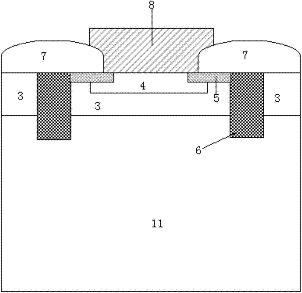
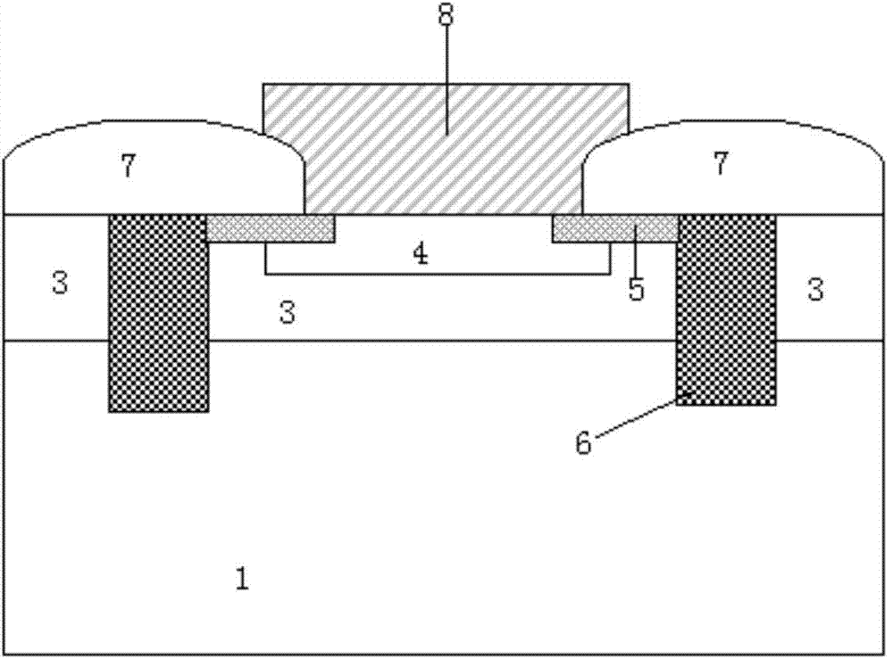
[0054] Prepare a piece of lightly doped substrate material with vapor phase doping or neutron irradiation, and select different doping concentrations or resistivities for the substrate material according to different withstand voltage requirements of IGBT devices. The front IGBT process is carried out on the substrate material. The main processes include: the production of the voltage-resistant ring and the field plate, the production of the Trench trench gate, the production of the conduction channel and the P-type collector layer, and the production of the emitter or source region. fabrication, fabrication of front contact holes, metal, passivation layers (eg figure 1 shown).

[0055] (2) After the front process is c

Embodiment 2

[0073] In this embodiment, the advanced backside process manufacturing method for improving the performance of the planar gate field termination type IGBT has the following steps:

[0074] (1) Carry out the front process of IGBT according to the conventional process

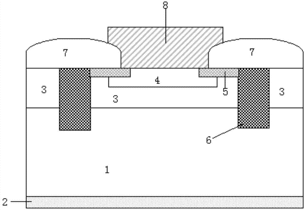
[0075] Prepare a piece of lightly doped substrate material with vapor phase doping or neutron irradiation, and select different doping concentrations or resistivities for the substrate material according to different withstand voltage requirements of IGBT devices. The front IGBT process is carried out on the substrate material. The main processes include: the production of the voltage-resistant ring and the field plate, the production of the planar gate, the production of the conduction channel and the P-type collector layer, and the production of the emitter or source region. , fabrication of front contact holes, metal, passivation layers (such as Figure 8 shown).

[0076] (2) After the front process is complete


PUM

PropertyMeasurementUnit
Depthaaaaaaaaaa
Depthaaaaaaaaaa
Depthaaaaaaaaaa

Abstract

The invention discloses an advanced back side process fabrication method for improving IGBT performance. The method comprises the steps that: (1) after an IGBT front side process is completed, the backside of a wafer is thinned, and then donor impurity ions are implanted into the back side of the wafer; (2) laser annealing is conducted to the back side of the wafer to activate the donor impurity ions implanted in the back side, so that an N type buffer layer serving as a field stop is formed; (3) acceptor impurity ions are implanted into the back side of the wafer; (4) laser annealing is conducted to the back side of the wafer to activate the acceptor impurity ions implanted in the back side, so that a P type collector layer serving as a collector is formed. By means of the method, the better 'figure of merit' matching between the pressure endurance and pressure drop breakover of an IGBT is achieved, and due to the fact that the electric current density of the IGBT is increased, the device dimension of the IGBT can be decreased correspondingly, and it is achieved that the cost of the IGBT is reduced.

Description


Claims


Application Information

Patent Timeline
Owner SHANGHAI HUAHONG GRACE SEMICON MFG CORP
Why Eureka
Try Eureka