Booster circuit and method for improving programming accuracy of EEPROM

A boost circuit and memory technology, applied in static memory, read-only memory, information storage, etc., can solve the problems of large chip area, high chip cost, and low accuracy of fuse correction, achieving small chip area, low cost, The effect of correcting high precision

Active Publication Date: 2017-01-04
深圳市航顺芯片技术研发有限公司
View PDF3 Cites 4 Cited by
  • Summary
  • Abstract
  • Description
  • Claims
  • Application Information

AI Technical Summary

Benefits of technology

This invention relates to improving the efficiency or precision with which circuits are used for data transmission over communication networks such as wireless communications systems (WCS). By reducing its size while maintaining good performance at lower costs compared to traditional methods like wired connections, this technology will have more potential benefits across different industries including manufacturing companies that require precise control on electronic devices during production processes.

Problems solved by technology

This patented technical problem addressed in this patents relates to improving the efficiency and precision of an electrical non volatile random access memory (electronic flash). Current methods involve changing voltages applied during programming operations which requires expensive components like external power supplies and complicated circuits.

Method used


Image

  • Booster circuit and method for improving programming accuracy of EEPROM
  • Booster circuit and method for improving programming accuracy of EEPROM
  • Booster circuit and method for improving programming accuracy of EEPROM

Examples


Embodiment Construction

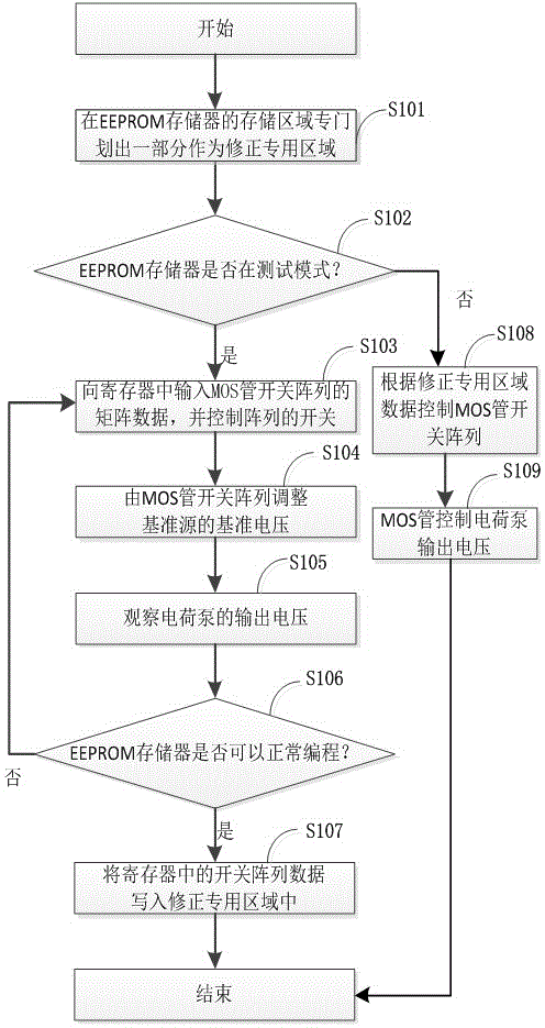
[0039] In order to make the purpose, technical solutions and advantages of the embodiments of the present invention more clear, the present invention will be further described below in conjunction with the accompanying drawings and specific implementation methods.

[0040] Attached below image 3 Embodiments of the present invention are described:

[0041] At present, EEPROM memory has entered the deep sub-micron era, and the complexity of EEPROM integration and process is getting higher and higher, especially for some high-performance new EEPROM memories, the requirements for programming voltage are also getting higher and higher.

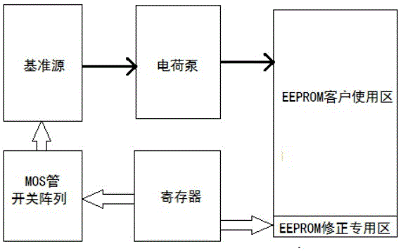
[0042] The invention makes full use of the feature that the EEPROM memory data can be stored for a long enough time when the chip is powered off, and a small part is specially designated in the EEPROM storage area as a special area for correction, and the area of ​​the designated part can be so small that it can be ignored. Such as figure 2 As sho


PUM


Abstract

The invention relates to a booster circuit and method for improving the programming accuracy of an EEPROM. The booster circuit comprises a register, an MOS tube switch array, a reference source, a charge pump and the EEPROM. The booster circuit fully utilizes the characteristic that the data of the EEPROM memorizer can be saved for enough long time when a chip is powered down to specially mark out a small part of an EEPROM storage area as a special correction area. The booster circuit has the advantages that a common register is firstly used for adjusting the accuracy of the booster circuit in a chip testing mode, the EEPROM can perform normal programming and stores the data in the register in the EEPROM special correction area when an accurate booster circuit voltage value is obtained. The booster circuit occupies small chip area and is low in cost. In addition, the register in the circuit can be repeated scanned, the digit can be corrected to be higher, and the correction accuracy is high.

Description


Claims


Application Information

Patent Timeline
Owner 深圳市航顺芯片技术研发有限公司
Why Eureka
Try Eureka