CMOS making method
A manufacturing method and fin technology, which are applied in semiconductor/solid-state device manufacturing, electrical components, circuits, etc., can solve the problems of reducing device reliability, cross-interference, unfavorable local device and CMOS hybrid integration in circuits, etc. cost effect
- Summary
- Abstract
- Description
- Claims
- Application Information
AI Technical Summary
Benefits of technology
Problems solved by technology
Method used
Image


Examples
Embodiment Construction
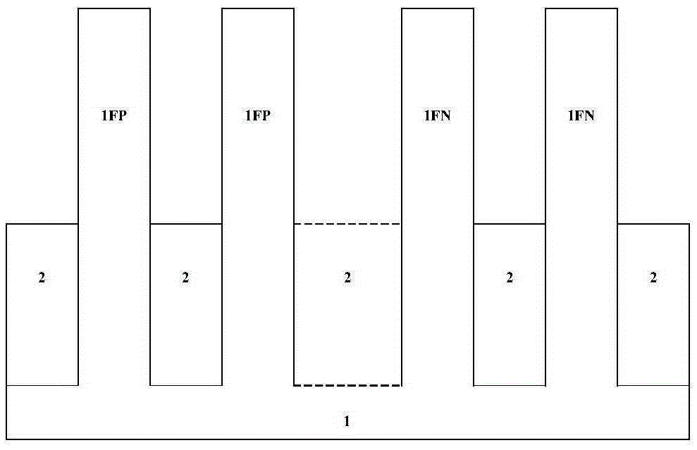
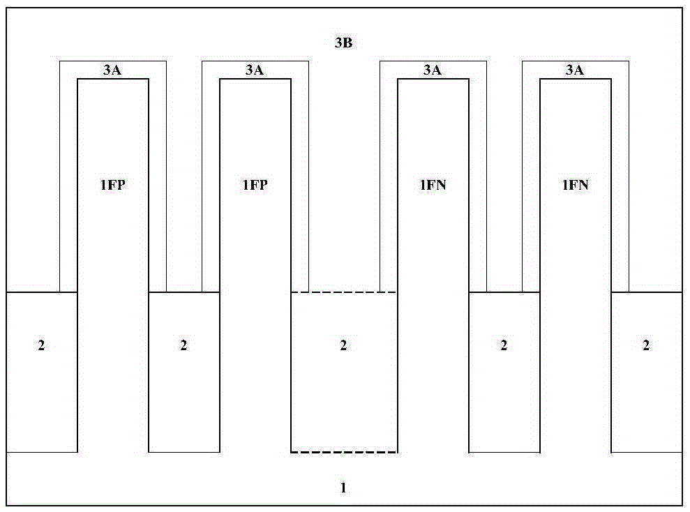
[0021] The features and technical effects of the technical solution of the present invention will be described in detail below with reference to the accompanying drawings and in conjunction with schematic embodiments, disclosing a high-mobility FET-type CMOS manufacturing method that improves device driving capability and reliability at low cost and high efficiency. It should be pointed out that similar reference numerals represent similar structures, and the terms "first", "second", "upper", "lower" and the like used in this application can be used to modify various device structures or manufacturing processes . These modifications do not imply spatial, sequential or hierarchical relationships of the modified device structures or fabrication processes unless specifically stated.
[0022] In particular, the following figure A is a cross-sectional view along a direction perpendicular to the channel (along the second direction), and certain figure B is a cross-sectional view along
PUM
 Abstract
Description
Claims
Application Information
 - R&D Engineer
- R&D Manager
- IP Professional
- Industry Leading Data Capabilities
- Powerful AI technology
- Patent DNA Extraction
Browse by: Latest US Patents, China's latest patents, Technical Efficacy Thesaurus, Application Domain, Technology Topic.
© 2024 PatSnap. All rights reserved.Legal|Privacy policy|Modern Slavery Act Transparency Statement|Sitemap