Reaction chamber and semiconductor processing device
A reaction chamber and chamber wall technology, which is applied in semiconductor/solid-state device manufacturing, metal material coating technology, ion implantation plating, etc., can solve problems such as poor contact, elastic fatigue, and poor deformation ability, and avoid The effect of sparking
- Summary
- Abstract
- Description
- Claims
- Application Information
AI Technical Summary
Problems solved by technology
Method used
Image

Examples
Embodiment Construction
[0029] In order for those skilled in the art to better understand the technical solution of the present invention, the reaction chamber and semiconductor processing equipment provided by the present invention will be described in detail below in conjunction with the accompanying drawings.
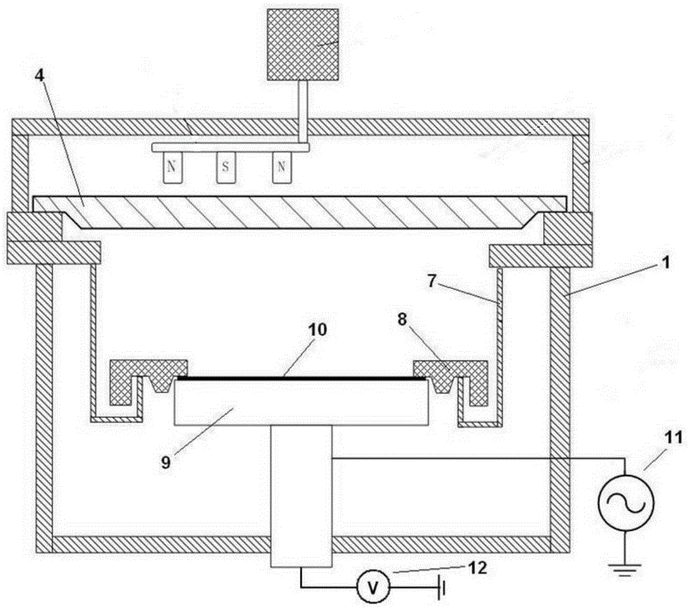
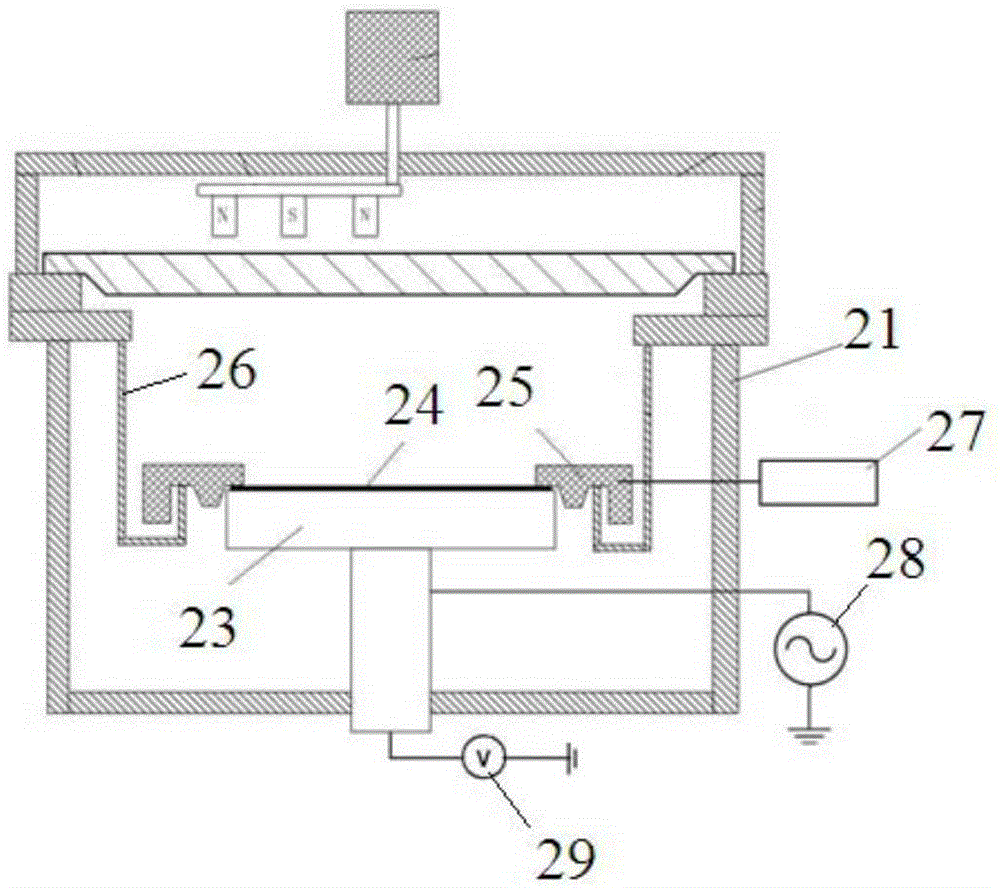
[0030] image 3 A cross-sectional view of a reaction chamber provided for an embodiment of the present invention. see image 3 , the reaction chamber 21 includes a base 23 , a snap ring 25 , a liner 26 , a detection device 29 and an adjustment device 27 . Wherein, the pedestal 23 is used for carrying the wafer 24, and the pedestal 23 is liftable, and when performing the process, the pedestal 23 rises to as high as image 3 Shown process position, now snap ring 25 utilizes self gravity to press the edge area of wafer 24, thereby wafer 24 is fixed on the base 23; Meanwhile, base 23 is connected with radio frequency power supply 28, and this radio frequency power supply 28 is carrying out Du
PUM
 Abstract
Description
Claims
Application Information
 - R&D Engineer
- R&D Manager
- IP Professional
- Industry Leading Data Capabilities
- Powerful AI technology
- Patent DNA Extraction
Browse by: Latest US Patents, China's latest patents, Technical Efficacy Thesaurus, Application Domain, Technology Topic.
© 2024 PatSnap. All rights reserved.Legal|Privacy policy|Modern Slavery Act Transparency Statement|Sitemap