LED device

A technology of LED devices and LED chips, which is applied in the direction of semiconductor devices, electrical components, circuits, etc., can solve the problems that LED devices cannot improve the consistency of light and color in barrier performance, so as to ensure the consistency of light and color, improve barrier performance, and improve matching effect

Pending Publication Date: 2017-12-22
GUANGZHOU HUMAN CHEM
View PDF0 Cites 1 Cited by
  • Summary
  • Abstract
  • Description
  • Claims
  • Application Information

AI Technical Summary

Benefits of technology

This patented technology allows for better control over how much insolation material (the sealing agent) should go into contact with an LED chip when it needs to protect from moisture or other factors like temperature changes without affects its function negatively. By controlling this distance, the manufacturer's products are more reliable and durable against damage caused by heat stress compared to traditional methods such as glue bonding alone.

Problems solved by technology

This patented technical problem addressed by this patents relates to improving the performance (convergence) and stability of LED lights when exposed to harsh environments such as outdoor sunlight without causing yellowish discolorations that could impact their appearance negatively.

Method used


Image

  • LED device
  • LED device
  • LED device

Examples


Embodiment 1

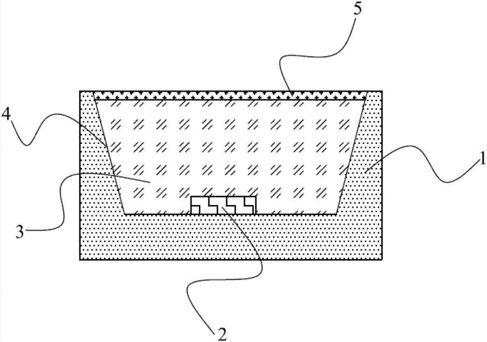
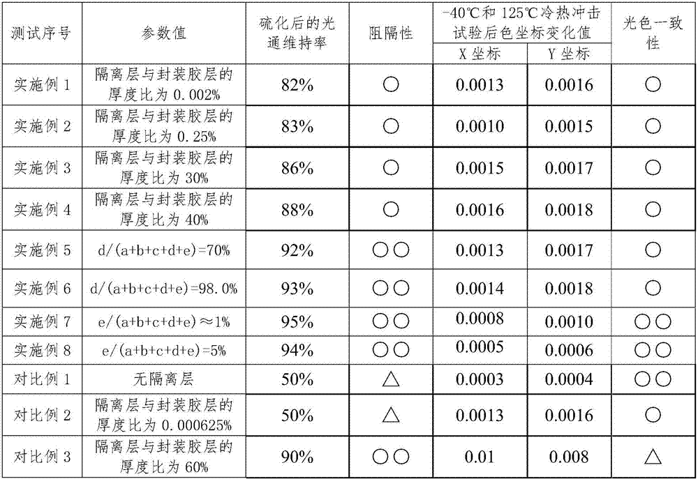
[0058] like figure 1 As shown, this embodiment provides an LED device, including a bracket 1, the bracket 1 is provided with an inverted trapezoidal groove 4, the surface of the groove 4 is provided with a silver-plated layer, the bottom of the groove 4 is provided with a bipolar chip, and the groove 4 is provided with a bipolar chip. 4. The inside is filled with an encapsulating adhesive layer 3 covering the bipolar chip, and the encapsulating adhesive layer 3 is organic silica gel mixed with yellow fluorescent powder. The surface of the encapsulation adhesive layer 3 is provided with an isolation layer 5, the isolation layer 5 is a polymer, and its molecular formula is (Ph 3 SiO 1 / 2 ) a (CH 3 SiO 3 / 2 ) b ((CH 3 ) 2 SiO 2 / 2 ) c (SiO 2 ) d , where a:b:c:d=10:25:35:35. The isolation layer 5 is coated on the upper surface of the encapsulation adhesive layer 3 by spraying. The isolation layer 5 is used to prevent the encapsulation adhesive layer 3 and the light ref

Embodiment 2

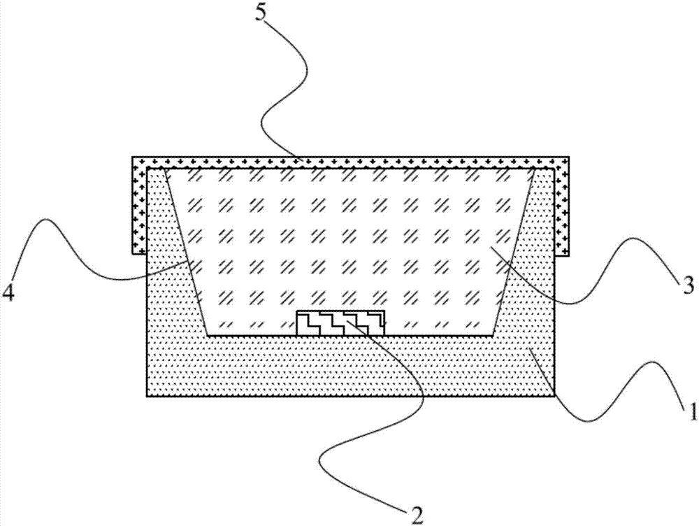
[0060] like figure 2 As shown, the difference between this embodiment and Embodiment 1 is that: the surface of the packaging adhesive layer 3 is provided with an isolation layer 5, and the isolation layer 5 extends to the upper surface and the outside of the bracket 1, so that there is no gap between the packaging adhesive layer 3 and the bracket 1. The thickness of the packaging adhesive layer 3 is 400000nm, the thickness of the isolation layer 5 is 1000nm, and the thickness ratio of the isolation layer 5 to the packaging adhesive layer 3 is 0.25%.

Embodiment 3

[0062] The difference between this embodiment and embodiment 1 lies in that the thickness of the packaging adhesive layer 3 is 600000 nm, the thickness of the isolation layer 5 is 180000 nm, and the thickness ratio of the isolation layer 5 to the packaging adhesive layer 3 is 30%.


PUM

PropertyMeasurementUnit
Thicknessaaaaaaaaaa
Thicknessaaaaaaaaaa
Thicknessaaaaaaaaaa

Abstract

The invention belongs to the field of lighting, and relates to an LED device. The LED device includes a bracket which is provided with a groove. A light reflecting layer is arranged on the surface of the groove. An LED chip is arranged at the bottom of the groove. The groove is filled with a packaging adhesive layer covering the LED chip. An isolating layer is arranged on the surface of the packaging adhesive layer. The isolating layer is used for stopping outside gas from corroding the light reflecting silver-plated layer through the packaging adhesive layer. The thickness ratio of the isolating layer to the packaging adhesive layer is 0.001-50%. The isolating layer can effectively prevent sulfide or oxygen from going into the LED device and reacting with the light reflecting silver-plated layer, can prevent the silver-plated layer from being corroded, and can significantly improve the light attenuation phenomenon of the LED device caused by corrosion of the light reflecting silver-plated layer. As the thickness ratio of the isolating layer to the packaging adhesive layer of the LED device is within a certain range, the isolating layer will be neither stripped nor cracked in the long-term hot and cold impact aging process, and the light color change of the LED device is very small.

Description


Claims


Application Information

Patent Timeline
Owner GUANGZHOU HUMAN CHEM
Why Eureka
Try Eureka