Detection device of chip for electronic equipment

A technology of electronic equipment and detection devices, applied in measuring devices, material analysis through optical means, instruments, etc., can solve the problems of inability to accurately photograph chips, inconvenient removal of chips, and inability to detect chips, etc., to solve the problem of inability to accurately photograph integrated chips , improve the versatility, and solve the effect of inconvenient removal

Pending Publication Date: 2020-09-04
JIANGSU A KERR BIOLOGICAL RECOGNITION TECH CO LTD
View PDF4 Cites 1 Cited by
  • Summary
  • Abstract
  • Description
  • Claims
  • Application Information

AI Technical Summary

Benefits of technology

This technology allows an improved way to check if multiple types of devices are being used together without having them all mixed up or requiring manual interference from others during testing process. It also includes features like moving the chip into collector before test results become available on it's screen. Additionally, this system uses cameras to capture images over time instead of relying solely upon visual inspection alone. Overall, these improvements improve the usability and effectiveness of electronic components such as smartphones.

Problems solved by technology

This patents describes an existing method for inspecting ICs used in various industries such as electronics manufacturing. These methods require manual labor and may result in low accuracy due to factors like variations between individual dies being examined by each testing machine. Additionally, these techniques involve taking multiple images from one area where there could be issues affecting their quality control over subsequent areas that were previously analyzed.

Method used


Image

  • Detection device of chip for electronic equipment
  • Detection device of chip for electronic equipment
  • Detection device of chip for electronic equipment

Examples


Embodiment 1

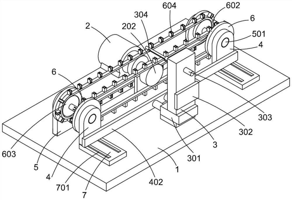
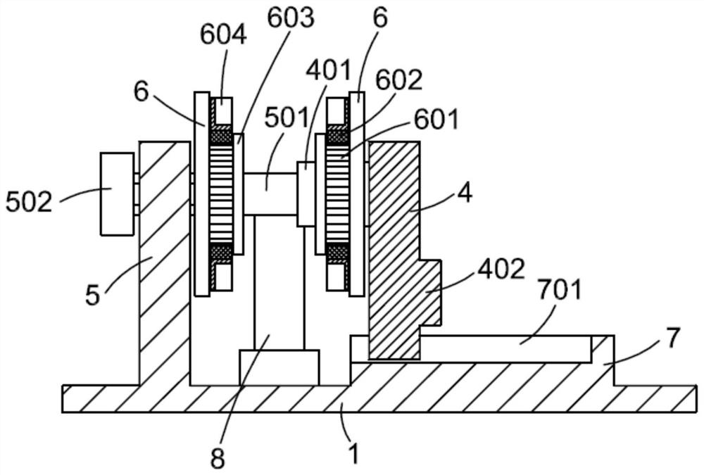
[0027] Embodiment 1: A detection device for chips used in electronic equipment, including a base plate 1, a motor 2 installed on the upper surface of the base plate 1, several fixed plates 5 arranged at intervals on the upper surface of the base plate 1, and several fixed plates 5 facing each other. The movable plate 4 provided, the motor 2 is installed on the outside of the fixed plate 5 or the movable plate 4, a slide plate 7 is arranged between the base plate 1 and the movable plate 4, and the lower surface of the movable plate 4 is movably installed on the on the slide plate 7, so that the movable plate 4 can move towards or away from the fixed plate 5;

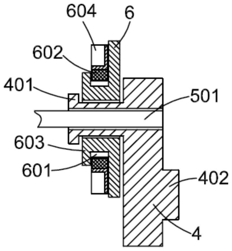
[0028] A limit shaft 501 is connected between the fixed plate 5 and the movable plate 4 which are arranged oppositely. On the side surface of the movable plate 4 close to the fixed plate 5, there is a convex tube 401 facing the fixed plate 5. The central opening of the convex tube 401 is There is a through hole for the limit

Embodiment 2

[0032] Embodiment 2: A detection device for chips used in electronic equipment, including a base plate 1, a motor 2 installed on the upper surface of the base plate 1, several fixed plates 5 arranged at intervals on the upper surface of the base plate 1, and several fixed plates 5 facing each other. The movable plate 4 provided, the motor 2 is installed on the outside of the fixed plate 5 or the movable plate 4, a slide plate 7 is arranged between the base plate 1 and the movable plate 4, and the lower surface of the movable plate 4 is movably installed on the on the slide plate 7, so that the movable plate 4 can move towards or away from the fixed plate 5;

[0033] A limit shaft 501 is connected between the fixed plate 5 and the movable plate 4 which are arranged oppositely. On the side surface of the movable plate 4 close to the fixed plate 5, there is a convex tube 401 facing the fixed plate 5. The central opening of the convex tube 401 is There is a through hole for the limit


PUM


Abstract

The invention discloses a detection device of a chip for electronic equipment. The device comprises a bottom plate, a motor, a fixed plate and movable plates; a sliding plate is arranged between the bottom plate and the movable plates; the output end of the motor is connected with a rotating shaft; a main gear is mounted at one end of the rotating shaft; an auxiliary gear is mounted on the rotating shaft between the main gear and the motor; the fixed plate and the movable plate are each provided with a rotating disc; the rotating discs are in transmission connection with the auxiliary gear andthe main gear through clamping belts; a mounting clamping groove is formed in the outer wall of each clamping belt; the movable plates are connected through a push plate, and an installation frame isarranged on the outer side of the push plate; a first air cylinder and a second air cylinder are installed on the installation frame; a CCD camera is connected with a push rod of the second air cylinder; a material returning base is further installed on the bottom plate; a third air cylinder is installed on the material returning base; and a rubber strip is connected with the output end of the third air cylinder. The problems that chips of different specifications cannot be detected, the chips are inconvenient to take out, and the chips cannot be shot accurately are solved.

Description


Claims


Application Information

Patent Timeline
Owner JIANGSU A KERR BIOLOGICAL RECOGNITION TECH CO LTD
Why Eureka
Try Eureka