Differential driving circuit of floating isolation switch
A technology of isolation switch and differential drive, which is applied in the direction of electronic switches, electrical components, pulse technology, etc., can solve the problems of separate supply, contradiction, and loss of drive speed, and achieve the effects of easy integration, simplified system design, and high switching speed
- Summary
- Abstract
- Description
- Claims
- Application Information
AI Technical Summary
Benefits of technology
Problems solved by technology
Method used
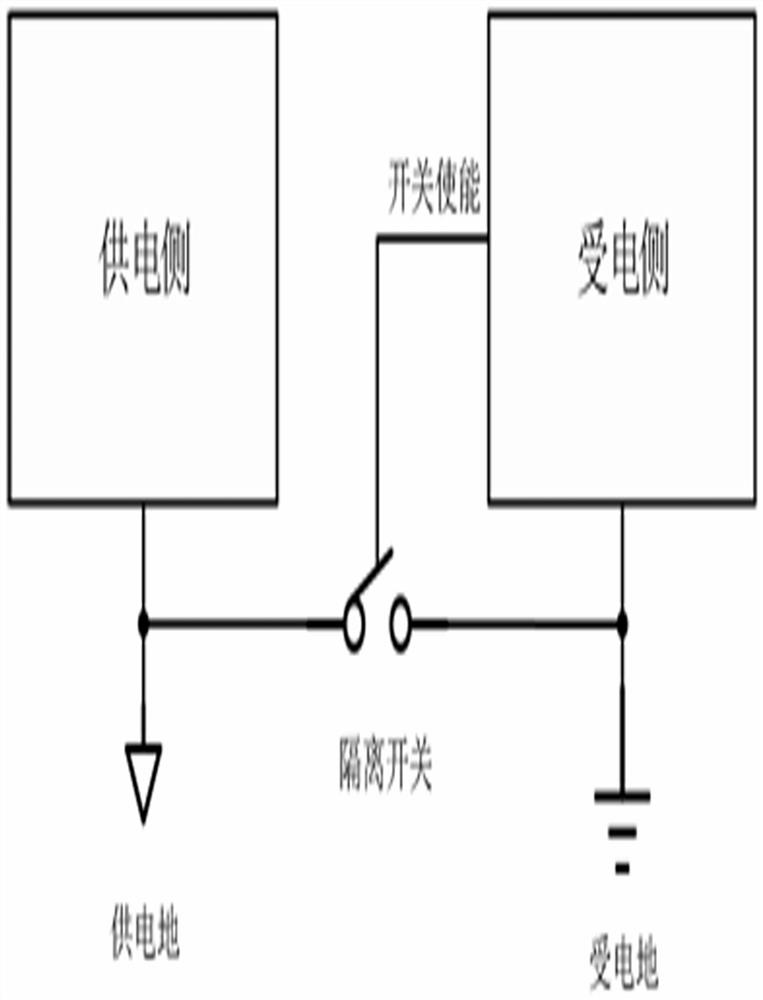
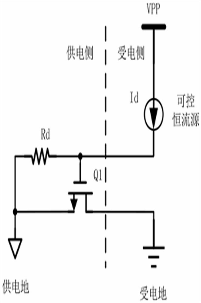
Image


Examples
Embodiment 1
[0044] see Figure 4 , Figure 4 A schematic diagram of a circuit for the present invention;
[0045] The specific process is as follows:
[0046] 1. When the receiving side controls the Ip current output and the In current has no output, the gate voltage Vgp of the isolating switch Q3 is pulled up, and the gate voltage Vgn of the isolating switch Q2 is pulled down by the opened isolating switch Q3, further closing the isolating switch Q2 , at this time the isolating switch Q1 and the isolating switch Q3 are in the open state, and the floating isolation is in the open state;
[0047] 2. When the power receiving side controls the In current output and the Ip current has no output, the gate voltage Vgn of the isolation switch Q2 is pulled high, and the gate voltage Vgp of the isolation switch Q3 is pulled down by the opened isolation switch Q2, further closing the isolation switch Q3 , at this time the isolation switch Q1 and the isolation switch Q3 are in the closed state, and
Embodiment 2
[0049] The polarity of Ip current and In current can control the closing and opening of the isolating switch, but it should be noted that the Ip current and In current need to be completely in the isolation switch Q3 gate voltage Vgp and the isolation switch Q2 gate voltage Vgn in the isolation switch Q2 and isolation switch Q3. After it is turned on, the output current is stopped, otherwise the gate voltage Vgp of the isolation switch Q3 and the gate voltage Vgn of the isolation switch Q2 will be charged to the VPP voltage, which may reach the gate withstand voltage limit of the isolation switch Q1, isolation switch Q2, and isolation switch Q3. Therefore, the Ip current and the In current are set to the voltage-limited constant-current source mode.
[0050] see Figure 5 , Figure 5 It is a schematic circuit diagram of a differential drive implementation shown in the present invention;
[0051] By increasing the voltage dividing resistor R1, the voltage dividing resistor R2, the
Embodiment 3
[0060] see Figure 6 , Figure 6 It is a specific circuit design diagram of the present invention;
[0061] The voltage dividing resistor R1 and the voltage dividing resistor R3 have the same resistance value, using a 100K resistor, and the voltage dividing resistor R2 and the voltage dividing resistor R4 have the same resistance value, using a 2M resistor, at this time the Vfp and Vfn voltages are the same;
[0062] The preset voltage Vd adopts diode D1 and diode D2 to generate a voltage drop, and adopts 0.7V;
[0063] Then, the final voltage of the gate voltage Vgn of the isolation switch Q2 is: Vd(1+R4 / R3) = 14.7V;
[0064] Then, the final voltage of the gate voltage Vgp of the isolation switch Q3 is: Vd(1+R2 / R1)=14.7V.
PUM
 Abstract
Description
Claims
Application Information
 - R&D Engineer
- R&D Manager
- IP Professional
- Industry Leading Data Capabilities
- Powerful AI technology
- Patent DNA Extraction
Browse by: Latest US Patents, China's latest patents, Technical Efficacy Thesaurus, Application Domain, Technology Topic.
© 2024 PatSnap. All rights reserved.Legal|Privacy policy|Modern Slavery Act Transparency Statement|Sitemap