M-bit optical delayer
A delayer and bit-bit technology, applied in the field of phased arrays, can solve problems such as delay errors and other wavelength intervals
- Summary
- Abstract
- Description
- Claims
- Application Information
AI Technical Summary
Problems solved by technology
Method used
Image

Examples
Embodiment 1
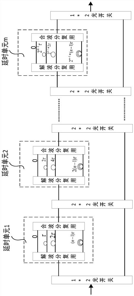
[0026] like figure 1 As shown, it is a schematic structural diagram of an m-bit optical delayer according to an embodiment of the present invention, a plurality of optical switches and a plurality of delay units constitute an m-bit optical delayer, and each delay unit includes a wavelength division multiplexing , wavelength division multiplexing and multi-channel delay line; the whole module includes a 1*2 optical switch, a 2*1 optical switch and multiple 2*2 optical switches. One 1*2 optical switch and one 2*1 optical switch are respectively located at both ends of the delayer. Multiple 2*2 optical switches are connected through multiple delay units. By controlling one 1*2 optical switch, The state of one 2*1 optical switch and multiple 2*2 optical switches controls the number of delay units that the optical signal passes through to form different delay paths.
[0027] The m-bit delayer inputs n optical carriers of different wavelengths at the same time, and passes through diff
PUM
 Abstract
Description
Claims
Application Information
 - R&D Engineer
- R&D Manager
- IP Professional
- Industry Leading Data Capabilities
- Powerful AI technology
- Patent DNA Extraction
Browse by: Latest US Patents, China's latest patents, Technical Efficacy Thesaurus, Application Domain, Technology Topic.
© 2024 PatSnap. All rights reserved.Legal|Privacy policy|Modern Slavery Act Transparency Statement|Sitemap