Semiconductor structure and forming method thereof
A semiconductor and graphics technology, applied in semiconductor devices, semiconductor/solid-state device manufacturing, electric solid-state devices, etc., can solve the problems of increasing the difficulty and complexity of integrated circuits, and achieve the improvement of optical proximity effect, graphics accuracy guarantee, and increase the process window effect
- Summary
- Abstract
- Description
- Claims
- Application Information
AI Technical Summary
Benefits of technology
Problems solved by technology
Method used
Image

Examples
Embodiment Construction
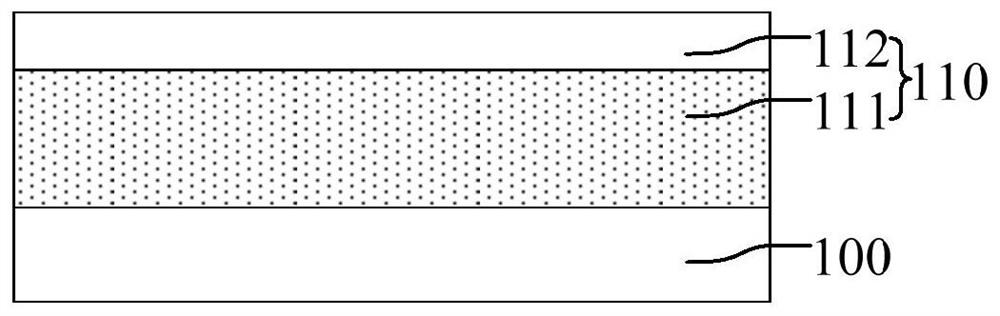
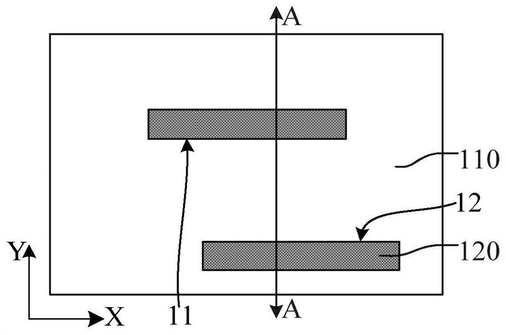
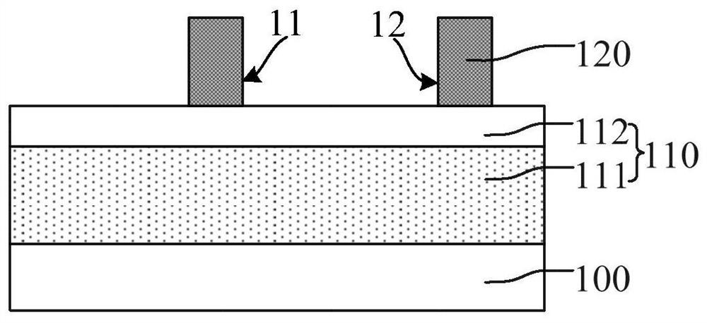
[0012] It can be seen from the background art that how to improve the matching degree between the pattern formed on the wafer and the target pattern becomes a challenge. Specifically, in the current back-end process, the patterning process of metal interconnection lines is very difficult and the process window is small.
[0013] For example, when the pattern of the interconnection pattern is complex, the photolithography process requires a large number of masks, which not only leads to high process costs, but also complicates the pattern of the mask, and the optical proximity correction process of the mask is also difficult. It has high difficulty, which leads to poor graphic accuracy and graphic quality of the formed interconnection lines, and even causes the problem of short-circuit (Bridge) of the interconnection lines at positions that do not need to be connected.
[0014] One method utilizes dummy interconnection lines (Dummy lines) to increase the window of the photolithogr
PUM
 Abstract
Description
Claims
Application Information
 - R&D Engineer
- R&D Manager
- IP Professional
- Industry Leading Data Capabilities
- Powerful AI technology
- Patent DNA Extraction
Browse by: Latest US Patents, China's latest patents, Technical Efficacy Thesaurus, Application Domain, Technology Topic.
© 2024 PatSnap. All rights reserved.Legal|Privacy policy|Modern Slavery Act Transparency Statement|Sitemap