ZnO Schottky diode

A technology of Schottky diodes and metal electrodes, which is applied in the direction of electrical components, circuits, semiconductor devices, etc., can solve the problems of low cut-off frequency, limited application occasions, large substrate series resistance, etc., and achieve high cut-off frequency, low price, The effect of strong radiation resistance

Inactive Publication Date: 2003-03-26
ZHEJIANG UNIV
View PDF0 Cites 1 Cited by
  • Summary
  • Abstract
  • Description
  • Claims
  • Application Information

AI Technical Summary

Problems solved by technology

This kind of Schottky diode has a large substrate series resistance

Method used


Image

  • ZnO Schottky diode
  • ZnO Schottky diode
  • ZnO Schottky diode

Examples


Embodiment Construction

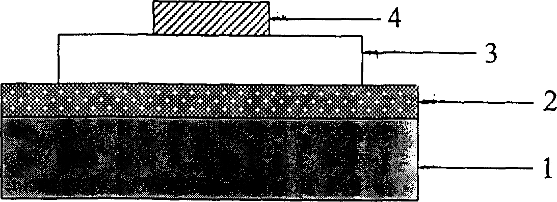
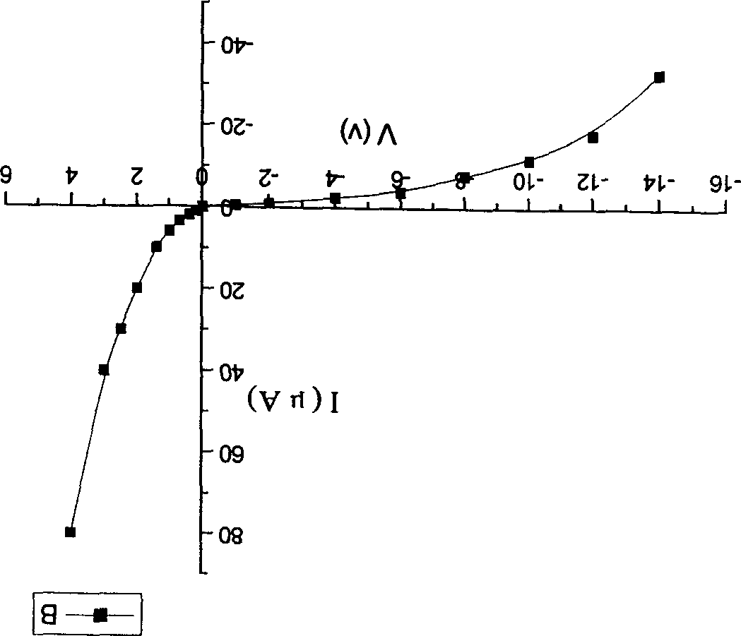
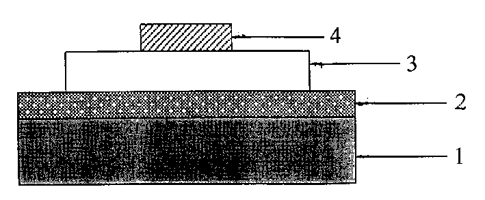
[0009] refer to figure 1 The ZnO Schottky diode of the present invention is formed by sequentially depositing a first metal electrode layer 2 , a ZnO crystal film epitaxial layer 3 and a second metal electrode layer 4 on the front surface of a substrate 1 from bottom to top. The substrate can be silicon, metal or glass. The thickness of the ZnO crystal film epitaxial layer is 0.3-1 μm. The first and second metal layers can be any metal. Generally, it is better to use aluminum for the first metal layer and platinum for the second metal layer. .

[0010] During preparation, the substrate is first cleaned according to conventional methods, and then the first metal layer, such as an aluminum film, is deposited on the substrate by vacuum evaporation, and then the ZnO crystal film layer is deposited on the aluminum film by magnetron sputtering deposition, and the A photolithographic process produces a second metal electrode layer, such as a platinum electrode, on the ZnO film.

[0


PUM

PropertyMeasurementUnit
Thicknessaaaaaaaaaa

Abstract

The first metal electrode layer, the ZnO crystal film epitaxial layer and the second metal electrode layer are deposited from the substrate to upper in sequence so as to form the ZnO schottky diode. Since the electrodes of the ohm contact and the Schottky contact are located at the two sides of the epitaxial layer directly, the too large series resistance caused by the substrate and resulted in idealization factor on the high side of the parts can be avoided. Thus, it is good for increasing the cut-off frequency. The ZnO film is adopted in the invention so as to provide the features of abundant material, low cost, suitable to the work in high temperature and high frequency as well as high radiation hardening. Moreover, there are low of substrates suitable for ZnO film to be deposited, making the design flexible and the technique simple.

Description


Claims


Application Information

Patent Timeline
Owner ZHEJIANG UNIV
Why Eureka
Try Eureka