Manufacturing method of film transistor matrix substrate

A technology of a thin film transistor and a manufacturing method, which is applied in the field of manufacturing a thin film transistor matrix substrate, can solve the problems of difficult control and difficulty in the actual process, and achieve the effects of reducing photocurrent generation, reducing film thickness, and reducing damage

Inactive Publication Date: 2006-06-28
AU OPTRONICS CORP
View PDF0 Cites 5 Cited by
  • Summary
  • Abstract
  • Description
  • Claims
  • Application Information

AI Technical Summary

Problems solved by technology

Because there must be two different photoresist heights in the same area, the photoresist angle (taper angle) and the photoresist thickness h1 on the island semiconductor in the channel region will affect the result of subsequent etching, so the control of the

Method used


Image

  • Manufacturing method of film transistor matrix substrate
  • Manufacturing method of film transistor matrix substrate
  • Manufacturing method of film transistor matrix substrate

Examples


Embodiment Construction

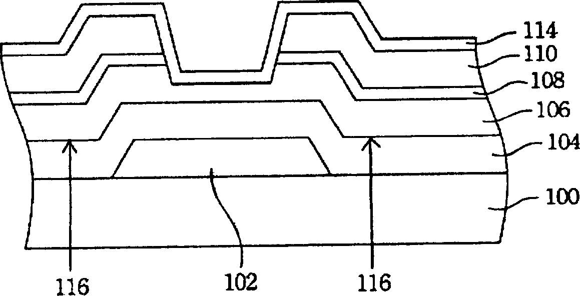
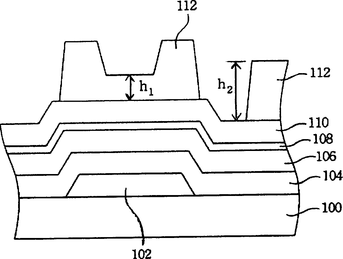
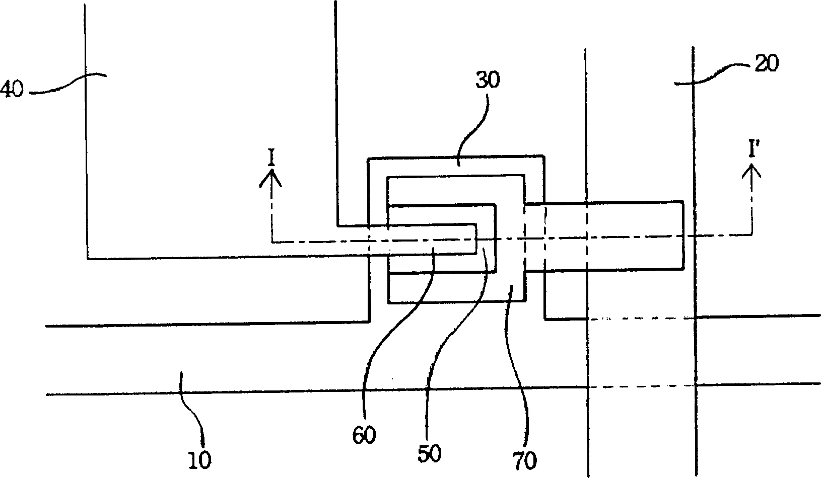
[0036] Please refer to image 3 , image 3 A schematic top view of the transistor array substrate (pixel unit structure) formed by a four-pass mask process according to a preferred embodiment of the present invention is shown. The transistor array substrate includes gate lines (scanning lines) 10 , signal lines or signal electrodes (data lines) 20 , gate electrodes 30 , pixel electrodes 40 , island-shaped semiconductors 50 , and source / drain electrodes 60 and 70 .

[0037] Please refer to Figure 4A to Figure 4D , Figure 4A to Figure 4D along image 3 As shown by the I-I' section line in the figure, it is a cross-sectional schematic diagram of the manufacturing process of the transistor array substrate formed by the four-pass mask process. Please refer to Figure 4A , on the transparent substrate 200, a conductive layer is defined by a mask process to form gate electrodes 30 and gate lines (scanning lines) (not shown). The transparent substrate 200 may be, for example, a


PUM


Abstract

A method for preparing base board with film transistor array includes forming island semiconductor above grid dielectric layer above grid electrode with grid width being greater than width of island semiconductor; forming lap hole on insulation layer covered above island semiconductor to expose partial island semiconductor; forming ohm contact by injecting ion on exposed island semiconductor surface and forming transparent conductive layer to clad above all structures; carrying out micro image etching process to define out source/ drain electrode, pixel electrode, grid electrode pad and signal electrode pad.

Description


Claims


Application Information

Patent Timeline
Owner AU OPTRONICS CORP
Why Eureka
Try Eureka