Plasma processing apparatus
a processing apparatus and plasma technology, applied in the direction of plasma technique, chemical vapor deposition coating, coating, etc., can solve the problems of above-described prior-art plasma generator, unstable discharge, damage to processing objects, etc., and achieve the effect of facilitating plasma generation in the plasma processing space, stable discharge, and low running cos
- Summary
- Abstract
- Description
- Claims
- Application Information
AI Technical Summary
Benefits of technology
Problems solved by technology
Method used
Image

Examples
first embodiment
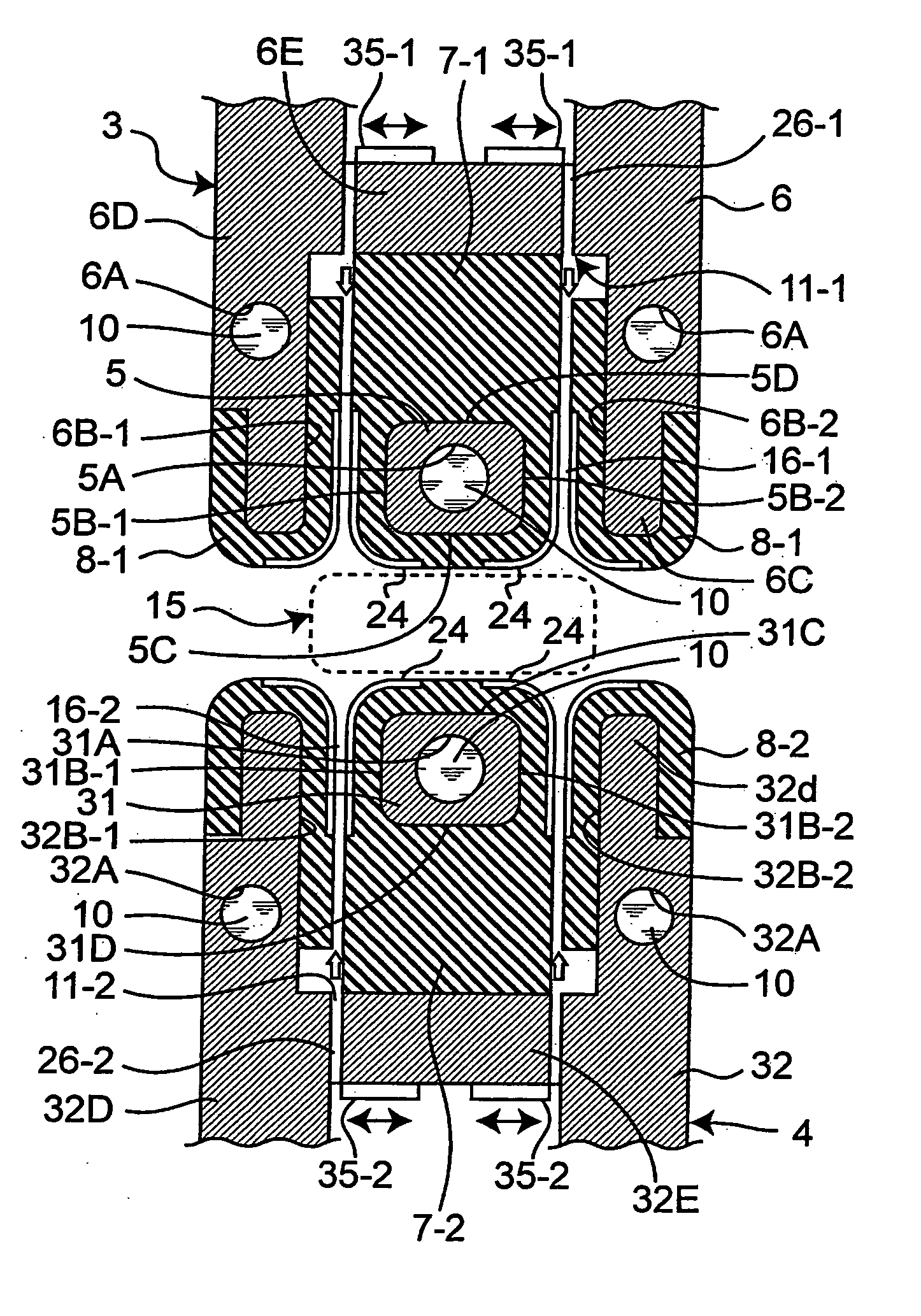
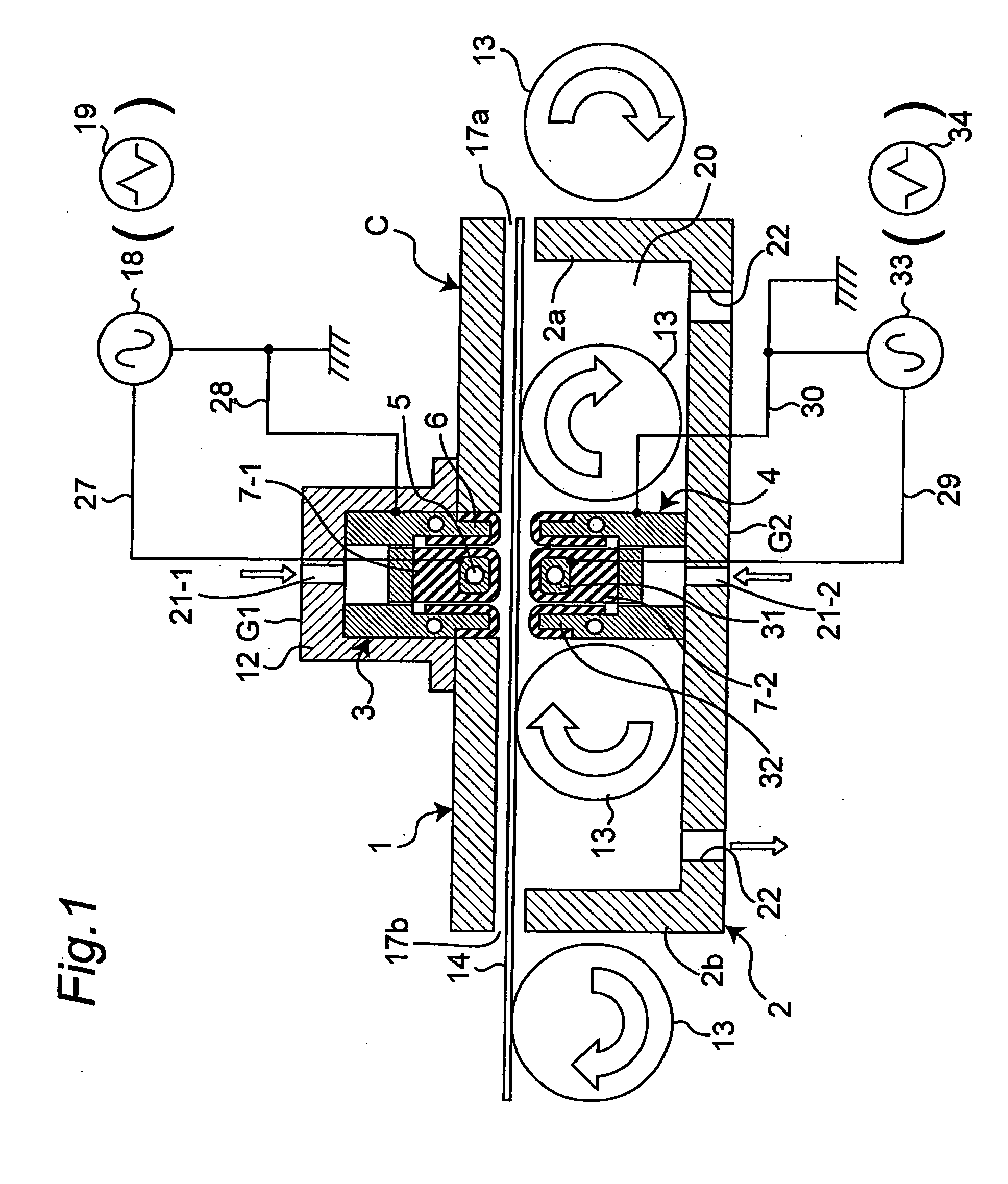
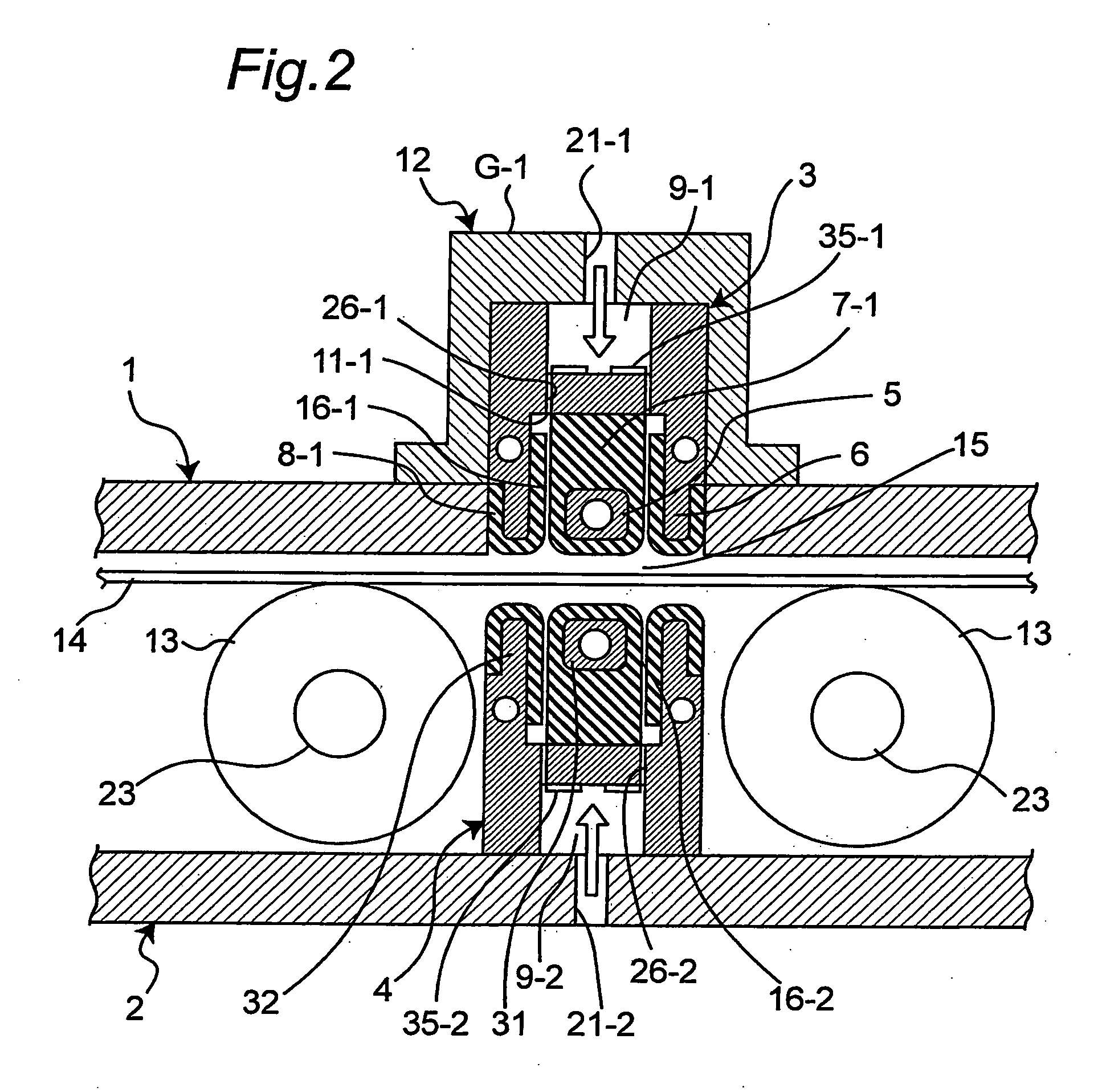
[0082]FIG. 1 shows a first embodiment of the plasma processing apparatus of the present invention. FIG. 1 is a side sectional view showing a cross section obtained by cutting the plasma processing apparatus by a plane vertical to a plate-shaped processing object 14 and which contains a line segment extending along a direction of conveyance of the processing object 14. FIG. 2 is an enlarged view showing a main part of the plasma processing apparatus. The processing object 14 is a semiconductor substrate as an example.
[0083] As shown in FIGS. 1 and 2, this plasma processing apparatus has a chamber upper part 1, a chamber lower part 2, an upper electrode unit 3 and a lower electrode unit 4. The chamber upper part 1 and the chamber lower part 2 constitute a chamber C. The chamber C has outlet and inlet 17a and 17b for the processing object 14 at both ends of the conveyance direction between the chamber upper part 1 and the chamber lower part 2.
[0084] The upper electrode unit 3 is fitted
second embodiment
[0139] Next, FIG. 8 shows a second embodiment of the plasma processing apparatus of the invention. The second embodiment differs from the foregoing first embodiment in that a lower electrode unit 50 is provided in place of the lower electrode unit 4. The lower electrode unit 50 is connected to the ground by an electric path 30.
[0140] The lower electrode unit 50 has a main electrode 51, and a fore end portion 51A of the main electrode 51 is covered with a dielectric portion 53. The fore end portion 51A has an opposing face 51C opposed to an opposing face 5C of the main electrode 5.
[0141] In FIG. 9, one example of RF voltage waveform given to the main electrode 5 by the RF power supply 18 is shown by numeral 42. The second embodiment is similar to the foregoing first embodiment in basic operations except that the lower electrode unit 50 is grounded. This second embodiment is suitable for cases where a rear face 14A of the processing object 14 does not need to be processed, producing ad
third embodiment
[0142] Next, FIG. 10 shows a third embodiment of the plasma processing apparatus of the invention. The third embodiment differs from the foregoing first embodiment in that a dielectric spray deposit 61 on a surface of the main electrode 5 and a dielectric spray deposit 62 is formed on a surface of the main electrode 31. The first dielectric portion 7-1 covers the dielectric spray deposit 61, and the first dielectric portion 7-2 covers a dielectric spray deposit 62.
[0143] This third embodiment has the dielectric coat 61 formed on the opposing face 5C and side faces 5B-1, 5B-2 of the main electrode 5. Therefore, even when the first dielectric portion 7-1 is provided as a component independent of the main electrode 5 so that the dielectric coat 61 is overlaid with the first dielectric portion 7-1, a gap (space) formed between the main electrode 5 and the first dielectric portion 7-1 can be suppressed to a minimum. Also, the embodiment has the dielectric coat 62 formed on the opposing fac
PUM
| Property | Measurement | Unit |
|---|---|---|
| Length | aaaaa | aaaaa |
| Dielectric polarization enthalpy | aaaaa | aaaaa |
| Area | aaaaa | aaaaa |
Abstract
Description
Claims
Application Information
 - R&D Engineer
- R&D Manager
- IP Professional
- Industry Leading Data Capabilities
- Powerful AI technology
- Patent DNA Extraction
Browse by: Latest US Patents, China's latest patents, Technical Efficacy Thesaurus, Application Domain, Technology Topic.
© 2024 PatSnap. All rights reserved.Legal|Privacy policy|Modern Slavery Act Transparency Statement|Sitemap