Low-noise large-area photoreceivers with low capacitance photodiodes

a photodiode and large-area technology, applied in the field of semiconductor devices, can solve the problems of reducing the bandwidth of the photodiode, limiting the sensitivity of the overall system, and adding to the equivalent input current nois

Active Publication Date: 2012-02-23
DISCOVERY SEMICON
View PDF17 Cites 38 Cited by
  • Summary
  • Abstract
  • Description
  • Claims
  • Application Information

AI Technical Summary

Benefits of technology

The present invention relates to an improved method for detecting light signals by utilizing multiple pairs of photosensitive elements arranged in rows or columns. This technology can be used with different types of sensors such as photoelectric cells or CMOS image sensor arrays.

Problems solved by technology

This patent describes a problem where increasing the effective area of a quaternary photocathector without adding extra circuitry increases the size of the photodetector while reducing the required signal-to-noise ratio (SNR) of the sensor. Additionally, it suggests integrating multiple smaller photoelectric receivers into one chip to improve their performance.

Method used


Image

  • Low-noise large-area photoreceivers with low capacitance photodiodes
  • Low-noise large-area photoreceivers with low capacitance photodiodes
  • Low-noise large-area photoreceivers with low capacitance photodiodes

Examples


Embodiment Construction

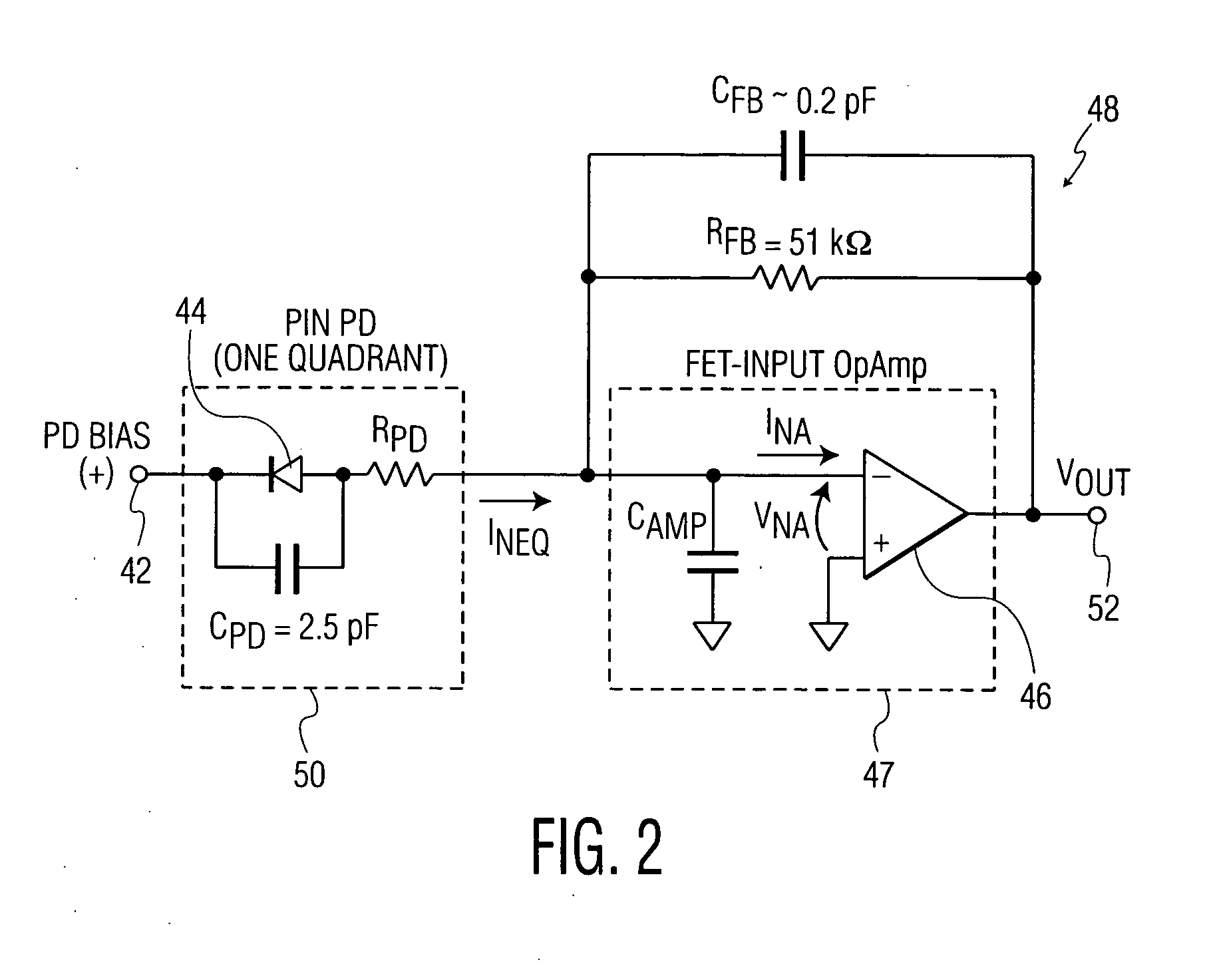
[0026]The present invention is directed to a quad photoreceiver based on low-capacitance quad photodiodes each followed by a transimpedance amplifier. In one embodiment of the present invention, there is provided a 1-mm-diameter InGaAs quad photodiode having 2.5-pF capacitance per quadrant. In conjunction with low-noise field effect transistor (FET)-input operational amplifiers, the associated low-capacitance quad photodiodes are each designed to provide a quad photoreceiver having an equivalent input current noise density of less than 3.2 pA / √Hz per quadrant up to a 3-dB bandwidth of ˜20 MHz. This constitutes up to ˜17-dB improvement in sensitivity over a quad photodiode having 20-pF capacitance per quadrant.

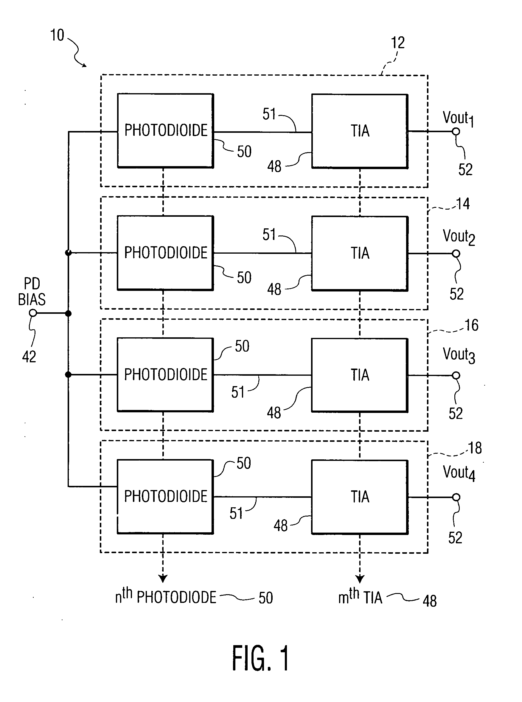
[0027]Referring to FIG. 1, a schematic block diagram of a quad photoreceiver 10 is shown for one embodiment of the present invention. The quad photoreceiver 10 includes four quadrants or sections 12, 14, 16, and 18 each having a photodiode 50 followed by a transimpedance amplifi


PUM


Abstract

A quad photoreceiver includes a low capacitance quad InGaAs p-i-n photodiode structure formed on an InP (100) substrate. The photodiode includes a substrate providing a buffer layer having a metal contact on its bottom portion serving as a common cathode for receiving a bias voltage, and successive layers deposited on its top portion, the first layer being drift layer, the second being an absorption layer, the third being a cap layer divided into four quarter pie shaped sections spaced apart, with metal contacts being deposited on outermost top portions of each section to provide output terminals, the top portions being active regions for detecting light. Four transimpedance amplifiers have input terminals electrically connected to individual output terminals of each p-i-n photodiode.

Description


Claims


Application Information

Patent Timeline
Owner DISCOVERY SEMICON
Why Eureka
Try Eureka