High frequency control of a semiconductor switch

A semiconductor and switching technology, applied in the control field of semiconductor switches, can solve the problems of inability to achieve switching speed, inappropriate switching frequency, etc.

Inactive Publication Date: 2006-10-18
KONINKLIJKE PHILIPS ELECTRONICS NV
View PDF0 Cites 16 Cited by
  • Summary
  • Abstract
  • Description
  • Claims
  • Application Information

AI Technical Summary

Benefits of technology

The present technology improves upon previous methods by allowing an electrical device (such as a power transistor) to quickly start up when it needs more voltage than usual before turning off again after being turned back on again. By doing this, there are fewer times during each cycle where they have to wait until their next turn around, resulting in faster response time compared to traditional ways like flipping them over one's shoulder.

Problems solved by technology

Technologies related to improving the performance of electronic devices during operation at high voltages include reducing their current consumption by optimizing how much electricity flows through them while still maintaining good electrical characteristics like reliability. To this end, various techniques may be applied including pulse width modulation technology, inductive chargers, and resonating gates.

Method used


Image

  • High frequency control of a semiconductor switch
  • High frequency control of a semiconductor switch
  • High frequency control of a semiconductor switch

Examples


Embodiment Construction

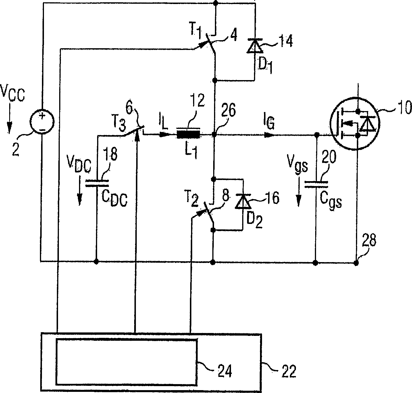
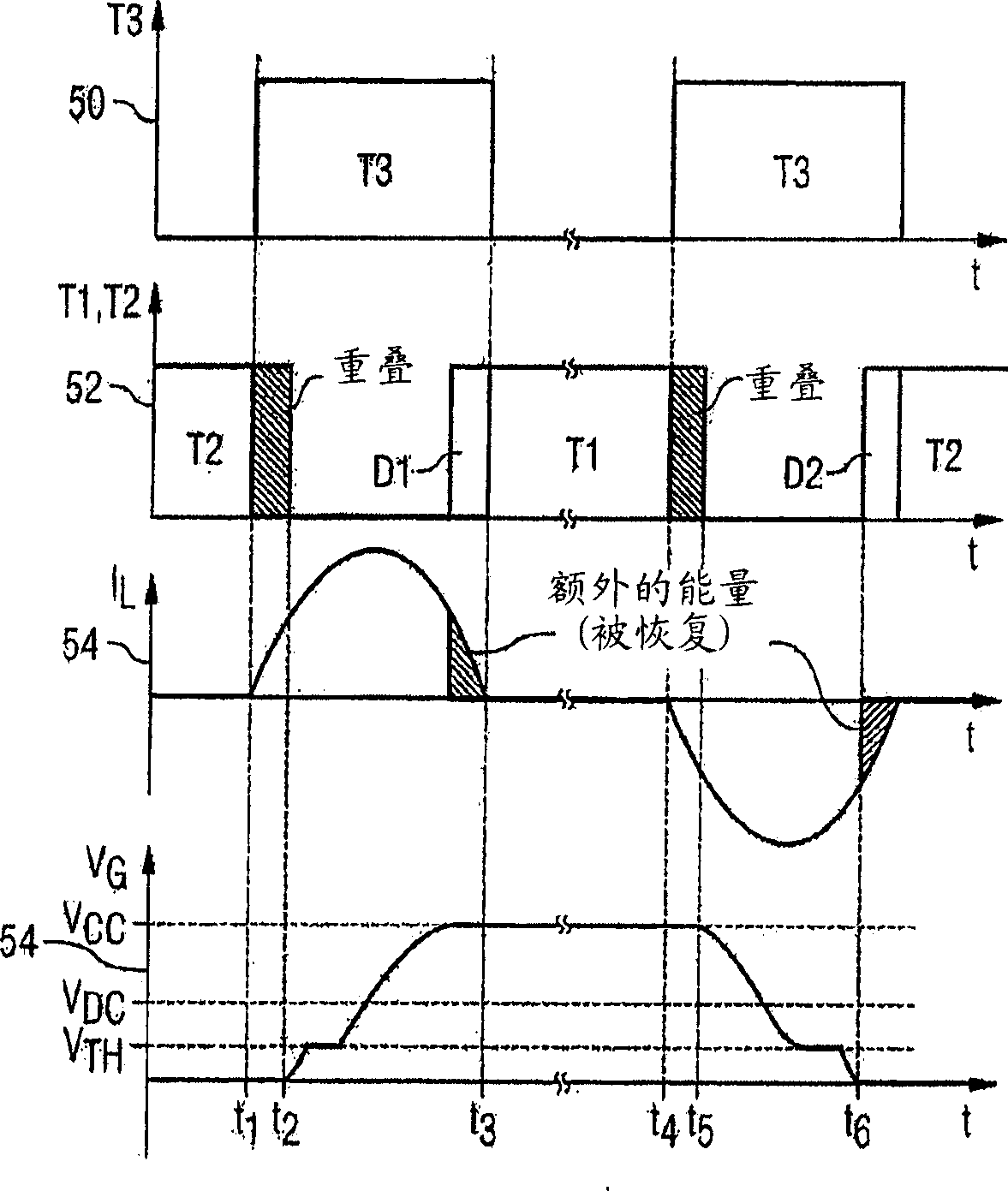
[0021] figure 1 A simplified circuit diagram of a resonant gate driver for driving a MOSFET 10, such as a power MOSFET, is shown. Although this exemplary embodiment of the invention is explained for driving a MOSFET 10, it should be understood that the invention is equally applicable to most types of voltage-controlled semiconductor switches, such as eg IGBTs. Furthermore, the present invention can also be applied to current controlled semiconductors such as bipolar transistors, thyristors and triacs. Reference numeral 22 designates an exemplary embodiment of a control circuit for controlling the operation of the resonant gate drive circuit according to the method of the present invention.

[0022] figure 1 The reference number 2 in the designates the power supply, which generates the supply voltage V cc . at supply voltage V cc and the control terminal 26 of the MOSFET 10, i.e. the gate of the MOSFET 10, a first switch T denoted by the reference numeral 4 is provided 1 .


PUM


Abstract

A resonant gate drive circuit provides efficient switching of, for example, MOSFETs. However, the operation of resonant gate drive circuits often does not allow applications where high switching frequencies are required. According to the invention, a precharging of the inductance of the resonant gate drive circuit is performed. This allows highly efficient and fast MOSFET operation.

Description


Claims


Application Information

Patent Timeline
Owner KONINKLIJKE PHILIPS ELECTRONICS NV
Why Eureka
Try Eureka