Semiconductor integrated circuit device

Inactive Publication Date: 2003-09-18
RENESAS TECH CORP
View PDF4 Cites 8 Cited by
  • Summary
  • Abstract
  • Description
  • Claims
  • Application Information

AI Technical Summary

Problems solved by technology

As a result of the recent development in technologies for finer semiconductor processing, the number of transistors that can be integrated on a single chip in a semiconductor integrated circuit device has drastically increased, which in turn causes increase of power consumption.
The reasons for using the power supply voltage VDDH for the interface portion are that: all transistors on each chip mounted on a board are not manufactured using the most advanced technologies for semiconductor processing; and a change in standards for the interface portion probably causes considerable confusion.
However, it is impossible to have a transistor(s) i

Method used


Image

  • Semiconductor integrated circuit device
  • Semiconductor integrated circuit device
  • Semiconductor integrated circuit device

Examples


Embodiment Construction

[0040] Below, preferred embodiments of the present invention will be discussed with reference to the accompanying drawings. It is noted that elements identical or similar to each other are denoted by the same reference character / numeral in the drawings.

[0041]

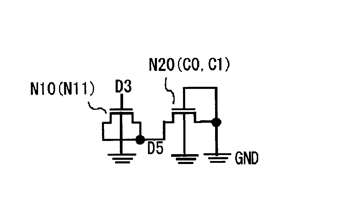
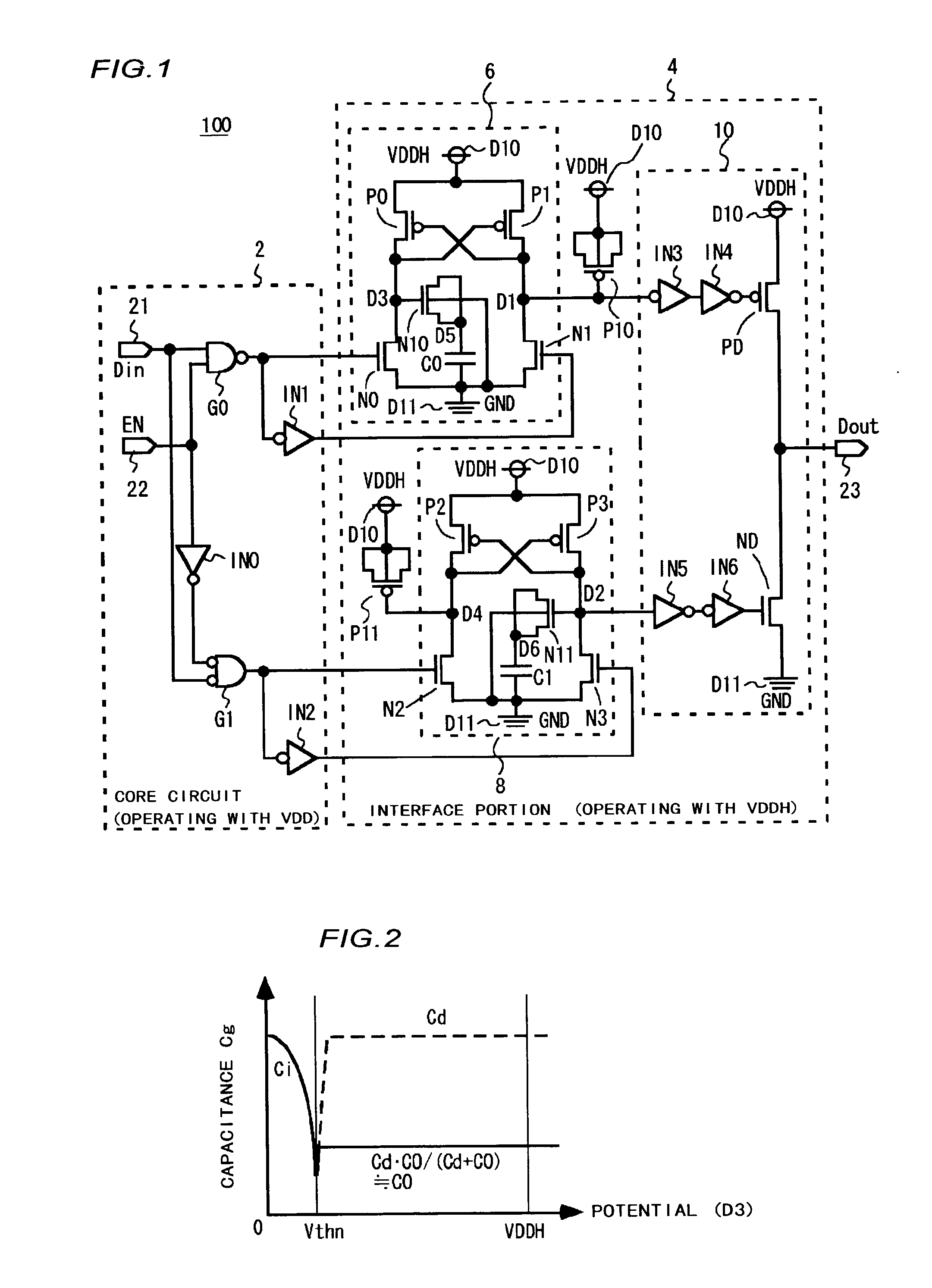
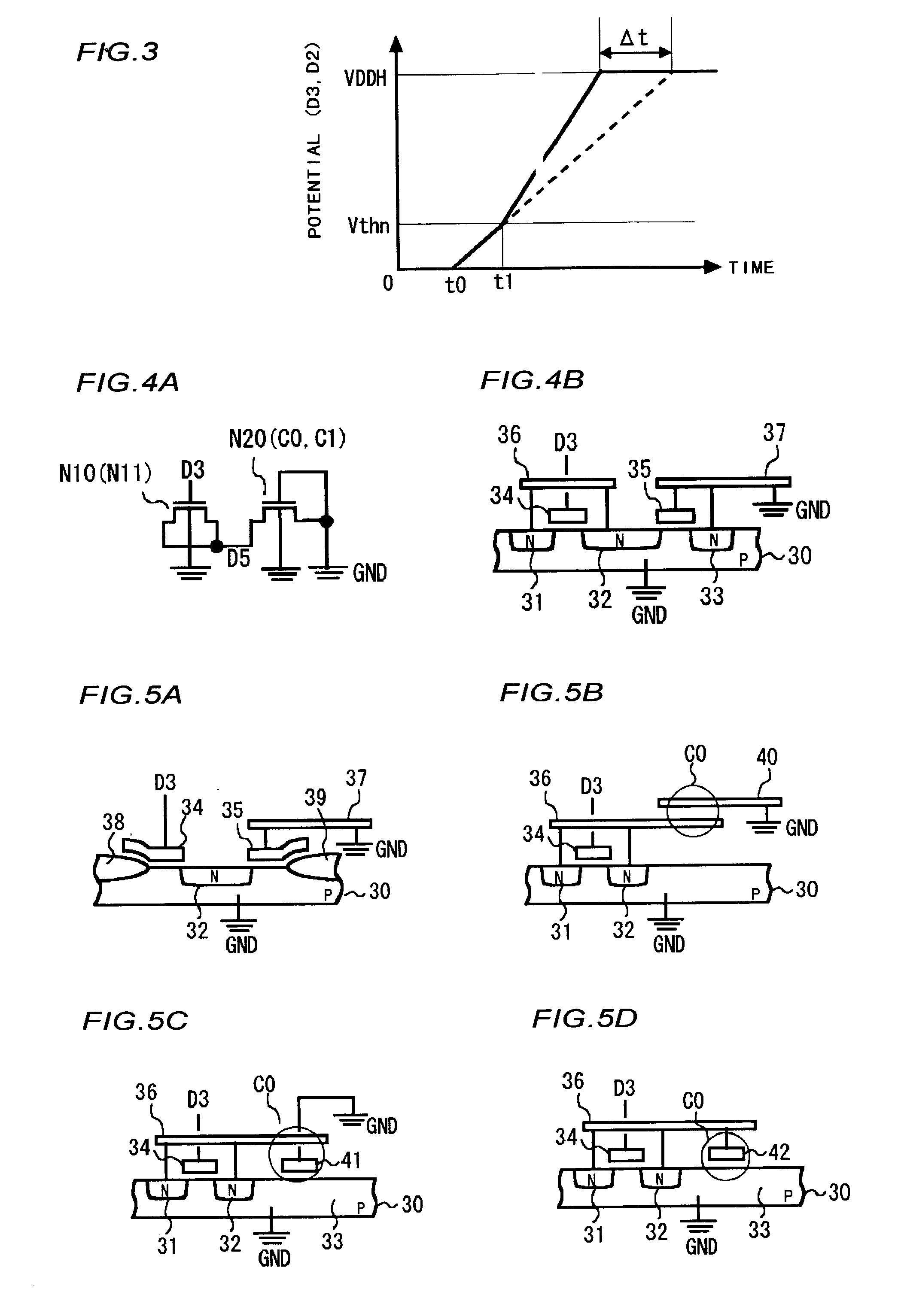
[0042] FIG. 1 is a circuit diagram showing a structure of a semiconductor integrated circuit device 100 according to a first preferred embodiment of the present invention. The semiconductor integrated circuit device 100 with a single semiconductor chip on which an integrated circuit is formed includes a core circuit 2 for implementing a primary function of the integrated circuit and an interface portion 4 for converting a digital signal Din generated in the core circuit 2 to a digital signal having a greater voltage amplitude than that of the signal Din, to provide the digital signal as a signal Dout to another semiconductor chip which is connected with a node 23.

[0043] The core circuit 2 is connected to a power node to which a


PUM


Abstract

A semiconductor integrated circuit device is provided, in which a node from which an output signal of a level shifter is sent can be initialized such that the potential thereof be set at a desired logic level at the time of power supply. The semiconductor integrated circuit device includes a level shifter 6 and two capacitors N10 and C0. The level shifter 6 receives an input signal and converts the received signal to a signal having a voltage amplitude greater than that of the received signal, then to provide the signal to a node D3. The capacitor N10 is connected to the node D3, and the capacitor C0 is connected in series with the capacitor N10. The capacitor N10 is formed of a MOS transistor having a gate connected to the node D3 and a source and a drain both connected to the capacitor C0.

Description


Claims


Application Information

Patent Timeline
Owner RENESAS TECH CORP
Why Eureka
Try Eureka