Method for manufacturing display device
a display device and manufacturing method technology, applied in the direction of optics, instruments, optical elements, etc., can solve the problems of limited regions where charged electrophoretic particles can migrate, the sealing material used to prepare the electrophoretic display device cannot be compatible with the dispersion medium, and the limited group of materials for forming the sealing layer is possibl
- Summary
- Abstract
- Description
- Claims
- Application Information
AI Technical Summary
Benefits of technology
Problems solved by technology
Method used
Image

Examples
example 1
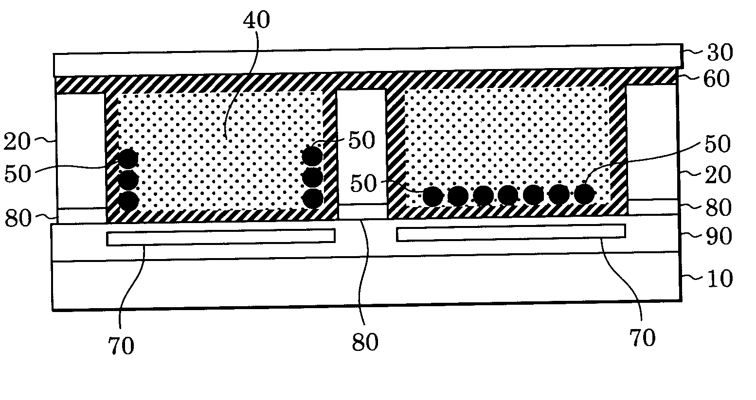
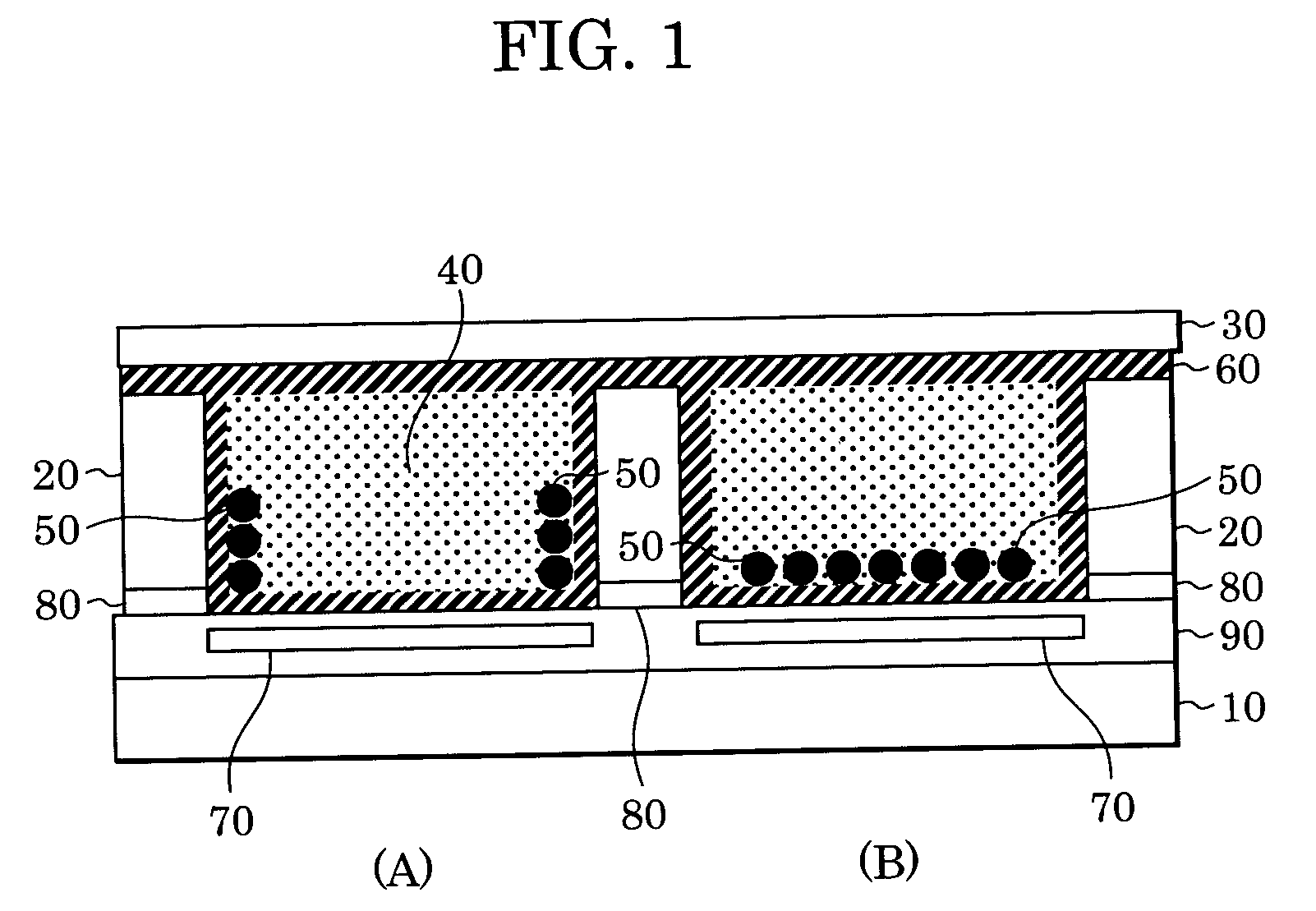
[0080] In this example, an electrophoretic display device shown in FIG. 1 was prepared. With reference to FIG. 1, the electrophoretic display device includes pixels, each surrounded by partitions 20, having a size of 100 μm square. The partitions 20 form a grid pattern and have a width of 8 μm and a height of 20 μm. First electrodes 70 are each placed directly below the corresponding pixels and connected to switching elements, which are not shown. A second electrode 80 is placed between a substrate 10 and the partitions 20 and commonly used to drive all the pixels.
[0081] A method for manufacturing the electrophoretic display device of this example will now be described.
[0082] The switching elements, the first electrodes 70, and an insulating layer 90 were formed on the substrate 10 by a known photolithographic process, the second electrode 80 was formed on the insulating layer 90, and the partitions 20 were then formed on the second electrode 80 by, for example, a known lithographic
example 2
[0090] A method for manufacturing an electrophoretic display device of this example includes the same steps as those described in Example 1, the steps being conducted prior to a step of forming partitions 20. In this example, the partitions 20 and an insulating layer 90 were surface-treated with a silane coupling agent (KBE-9007 manufactured by Shin-Etsu Chemical Co., Ltd.), terminated with an isocyanate group, by a known process.
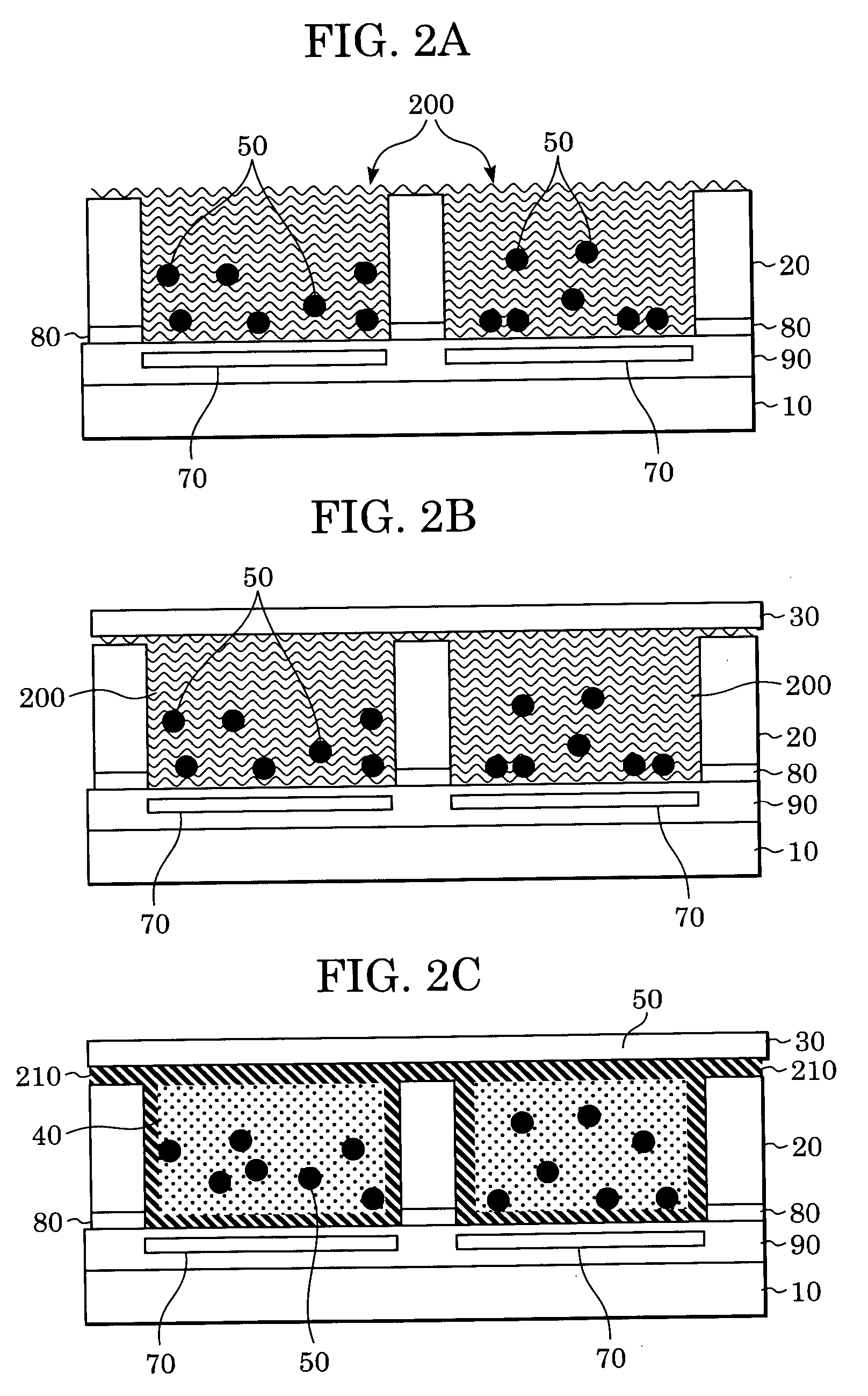
[0091] A dispersion 200 containing charged electrophoretic particles 50, a dispersion medium 40, and a sealing layer precursor 210 was packed in hollows defined by an insulating layer 90 and the partitions 20 as shown in FIG. 2A. In this example, the dispersion medium 40 was isoparaffin (Isopar™, manufactured by Exxon Mobil Corporation, having a density of 0.76) containing succinimide (OLOA™ 1200, manufactured by Chevron Chemical Company) acting as a charge control agent. The charged electrophoretic particles 50 were polymer beads which had an average particl
example 3
[0098] A method for manufacturing an electrophoretic display device of this example includes the same steps as those described in Example 1. The steps were conducted prior to a step of forming partitions 20. In this example, after the partitions 20 were formed, a dispersion 200 containing charged electrophoretic particles 50, a dispersion medium 40, and a sealing layer precursor 210 was packed in hollows defined by an insulating layer 90 and the partitions 20 as shown in FIG. 2A. The dispersion medium 40 was isoparaffin (Isopar™, manufactured by Exxon Mobil Corporation, having a density of 0.76) containing succinimide (OLOA™ 1200, manufactured by Chevron Chemical Company) acting as a charge control agent. The charged electrophoretic particles 50 were polymer beads which had an average particle size of about 1 to 2 μm, were made of a polystyrene-polymethylmethacrylate copolymer, and which contained carbon black.
[0099] The sealing layer precursor 210 contained 1H,1H,5H-octafluoropentyl
PUM
| Property | Measurement | Unit |
|---|---|---|
| Amphipathicity | aaaaa | aaaaa |
| Affinity | aaaaa | aaaaa |
Abstract
Description
Claims
Application Information
 - R&D Engineer
- R&D Manager
- IP Professional
- Industry Leading Data Capabilities
- Powerful AI technology
- Patent DNA Extraction
Browse by: Latest US Patents, China's latest patents, Technical Efficacy Thesaurus, Application Domain, Technology Topic.
© 2024 PatSnap. All rights reserved.Legal|Privacy policy|Modern Slavery Act Transparency Statement|Sitemap