Semiconductor memory device, system with semiconductor memory device, and method for operating a semiconductor memory device

Active Publication Date: 2006-07-20
POLARIS INNOVATIONS
View PDF4 Cites 3 Cited by
  • Summary
  • Abstract
  • Description
  • Claims
  • Application Information

AI Technical Summary

Benefits of technology

[0026] It is of advantage if the memory is a latency time register, in particular a CAS latency time register, and

Problems solved by technology

This delay results, for instance, from the time required by the sense amplifiers for amplifying the data supplied by the memory cells addressed by the word line.
The use of the above-mentioned

Method used


Image

  • Semiconductor memory device, system with semiconductor memory device, and method for operating a semiconductor memory device
  • Semiconductor memory device, system with semiconductor memory device, and method for operating a semiconductor memory device
  • Semiconductor memory device, system with semiconductor memory device, and method for operating a semiconductor memory device

Examples


Embodiment Construction

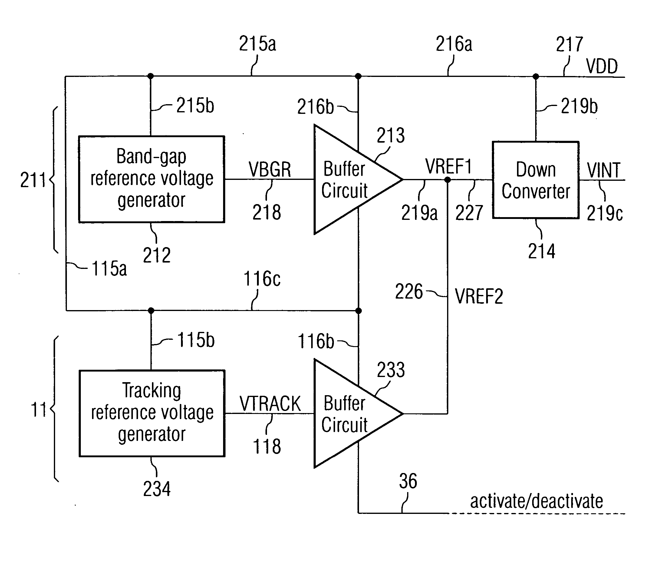
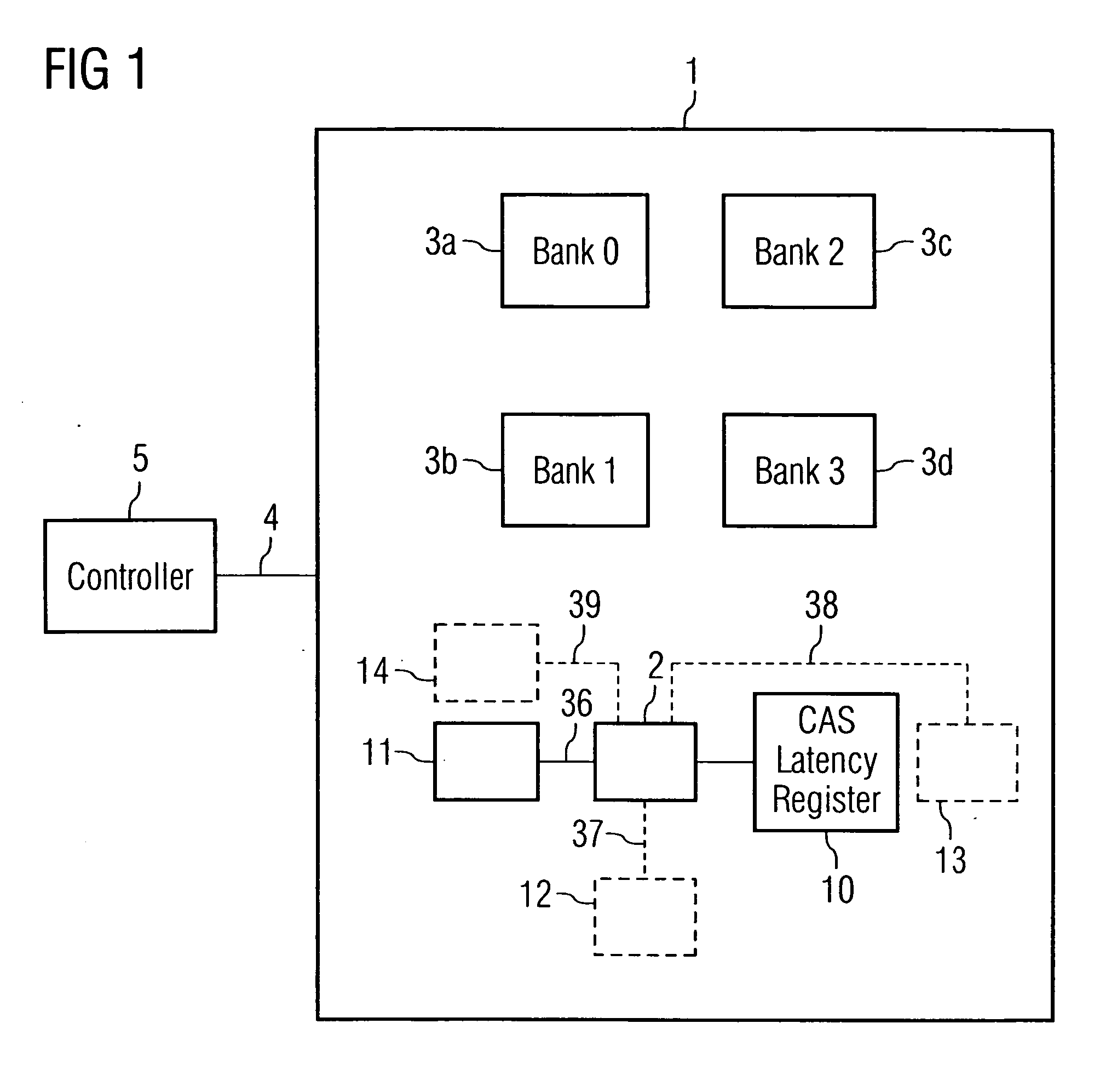
[0037]FIG. 1 shows a schematic representation of the structure of a semiconductor memory device 1 or semiconductor memory chip, respectively, and of a—central—memory device controller 5 according to an embodiment of the present invention.

[0038] The semiconductor memory device 1 may, for instance, be a table memory device based on CMOS technology, e.g. a RAM memory device (RAM Random Access Memory or read-write memory), in particular a SRAM memory device (SRAM=Static Random Access Memory) or a DRAM memory device (DRAM=Dynamic Random Access Memory or dynamic read-write memory) (e.g. a DDR-DRAM (DDR-DRAM=Double Data Rate DRAM).

[0039] In the semiconductor memory device 1, data may—after the input of a corresponding address—be stored under the respective address and be read out again under this address later.

[0040] The address may be input in several, e.g. two successive steps (e.g. first a row address (“row address”)—and possibly parts of a column address (“column address”)—, and then t


PUM


Abstract

The invention relates to a semiconductor memory device, a system with a semiconductor memory device, and a method for operating a semiconductor memory device, comprising the steps of reading out a data value, in particular a CAS latency time data value (CL) stored in a memory; activating or deactivating a device provided on said semiconductor memory device in support of a high speed operation, as a function of the data value (CL) stored.

Description


Claims


Application Information

Patent Timeline
Owner POLARIS INNOVATIONS
Why Eureka
Try Eureka