System, Masks, and Methods for Photomasks Optimized with Approximate and Accurate Merit Functions
- Summary
- Abstract
- Description
- Claims
- Application Information
AI Technical Summary
Benefits of technology
Problems solved by technology
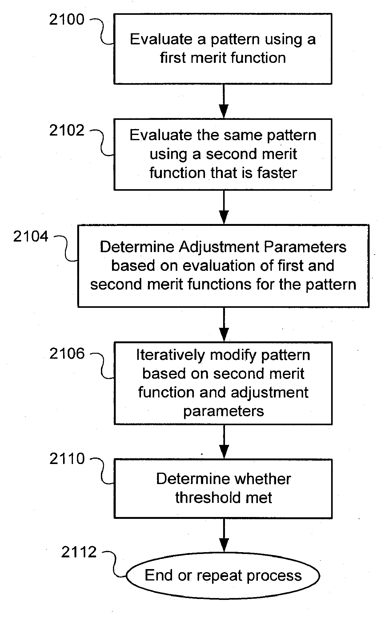
Method used
Image

Examples
Example
[0052] As understood herein, the term “wafer pattern” is understood to include any polygon (rectilinear or non-rectilinear) or other shape or pattern to be formed on a semiconductor or other material substrate, for example digital or analog circuit structures or interconnect.
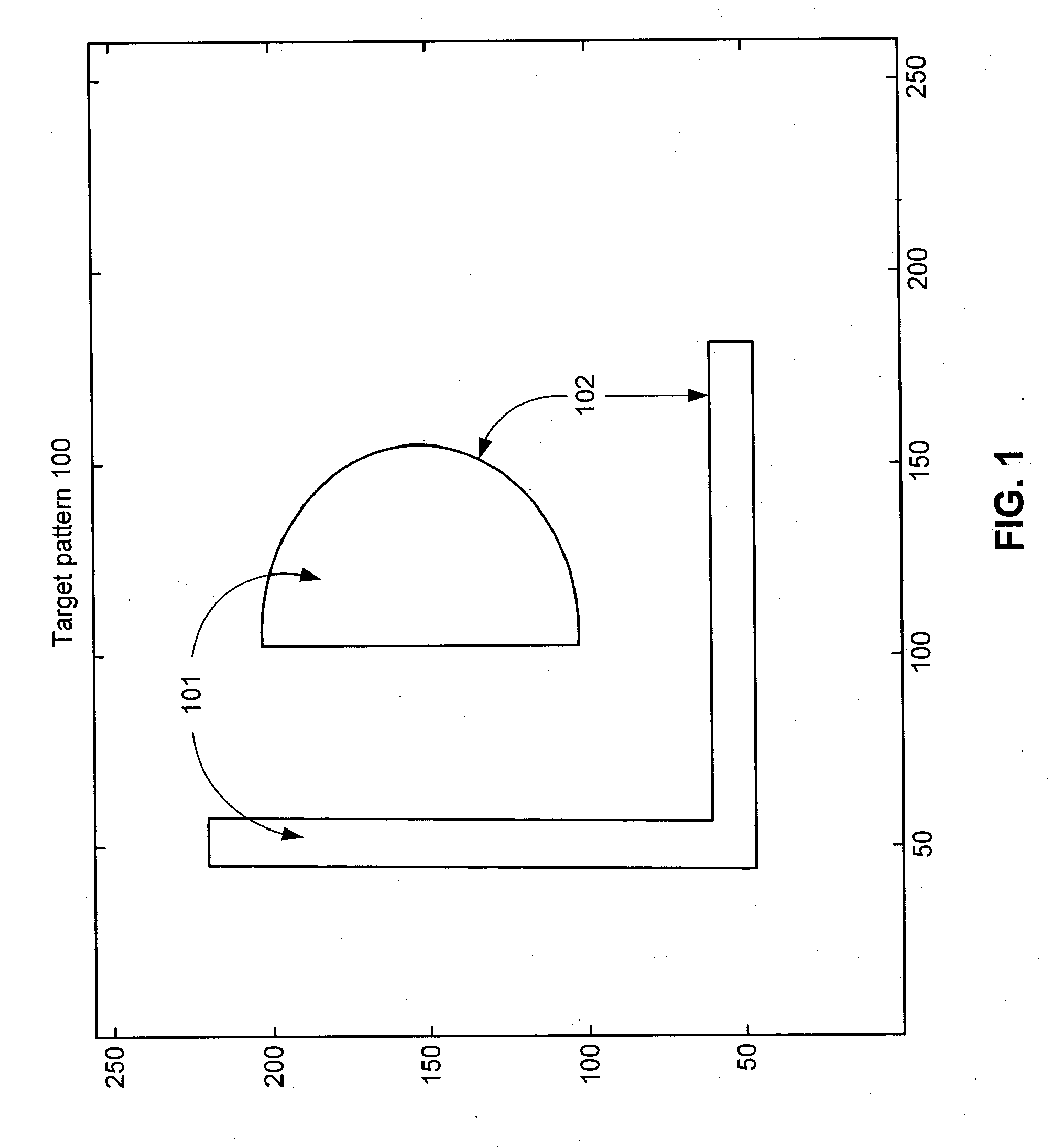
[0053]FIG. 1 is a diagram illustrating an example target pattern 100 to be printed on a wafer using a photolithography process. Target pattern 100 comprises regions 101 enclosed by contours 102. In an example embodiment, areas within regions 101 represent photoresist and the area outside regions 101 represents the absence of photoresist.
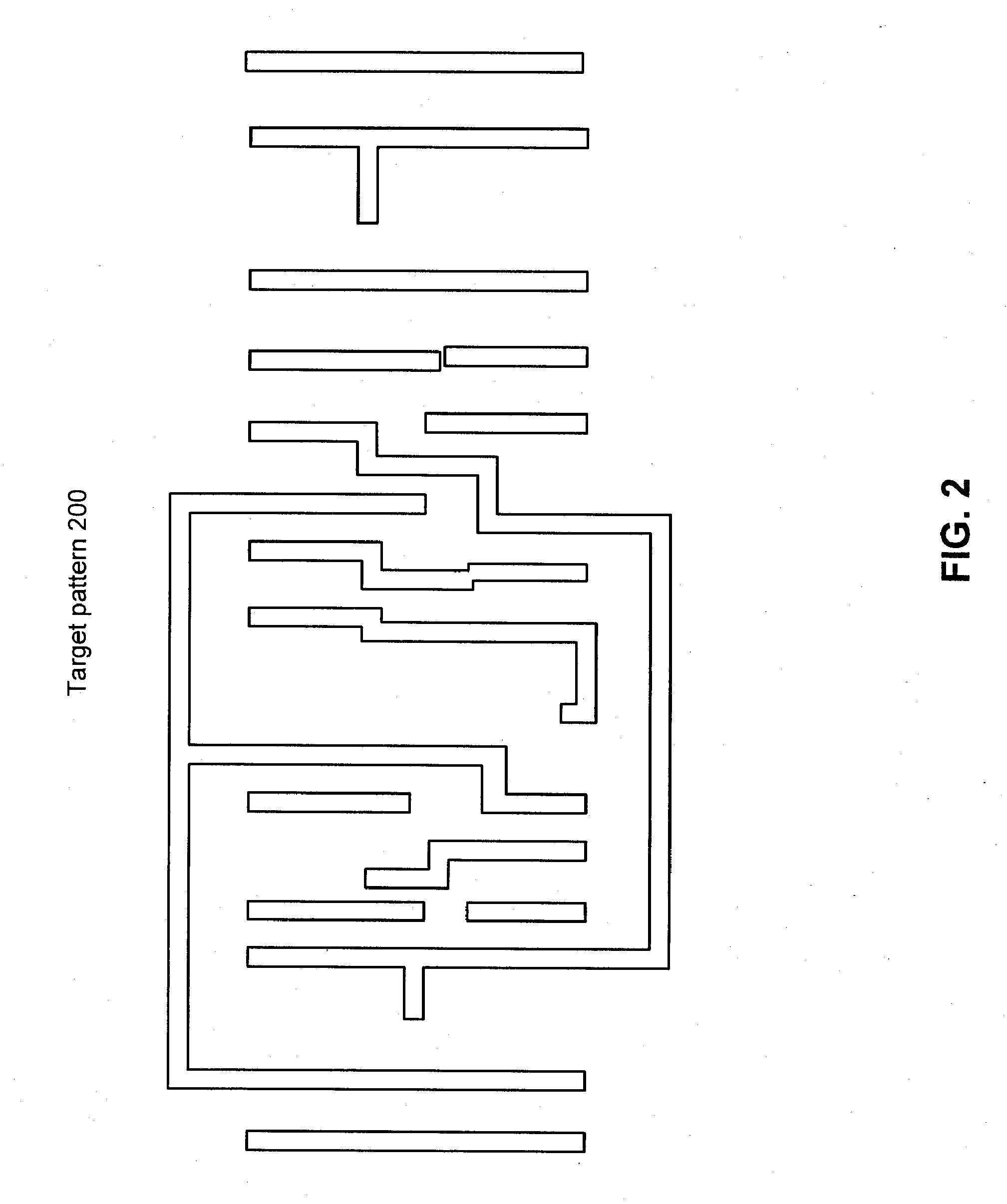
[0054]FIG. 2 is a diagram illustrating a more complex example target pattern 200 to be printed on a wafer using a photolithography process. The complexity of target pattern 200 is more illustrative of a pattern for representing an integrated circuit design.
[0055]FIG. 3 is a diagram illustrating a detail target pattern 300 from the example target pattern 200 of FIG. 2 to be printe
PUM
 Abstract
Description
Claims
Application Information
 - R&D Engineer
- R&D Manager
- IP Professional
- Industry Leading Data Capabilities
- Powerful AI technology
- Patent DNA Extraction
Browse by: Latest US Patents, China's latest patents, Technical Efficacy Thesaurus, Application Domain, Technology Topic.
© 2024 PatSnap. All rights reserved.Legal|Privacy policy|Modern Slavery Act Transparency Statement|Sitemap