Coupled lamb wave resonators filter
- Summary
- Abstract
- Description
- Claims
- Application Information
AI Technical Summary
Benefits of technology
Problems solved by technology
Method used
Image

Examples
Example
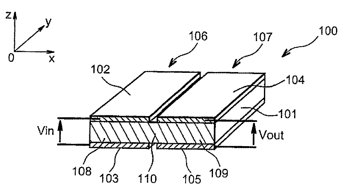
[0038]In this first embodiment, the coupled Lamb wave resonators filter 100 is made to obtain a narrow passband at the output centered around a central frequency equal to about
fc=cλc.
For example, in aluminium nitride fc is between about 100 MHz and 300 MHz, and c≈10000 m.s−1 for a symmetric Lamb wave of mode S0. When the central frequency goes outside this frequency range, the velocity c decreases due to frequency dispersion. This is done by sizing the two resonators 106, 107 such that the length of each is equal to about
λc2
for a central frequency fc. Thus, the lateral resonances of Lamb waves having a length equal to about λc are used to obtain a principal resonance with frequency fc. More generally, the resonator lengths 106 and 107, in other words the lengths of electrodes 102 to 105 and / or resonant layers 108 and 109 along the x axis in FIG. 1, can be equal to about
kλc2,
where k is a non-zero natural integer number. The variable k is preferably odd.
[0039]In this first embodiment,
Example
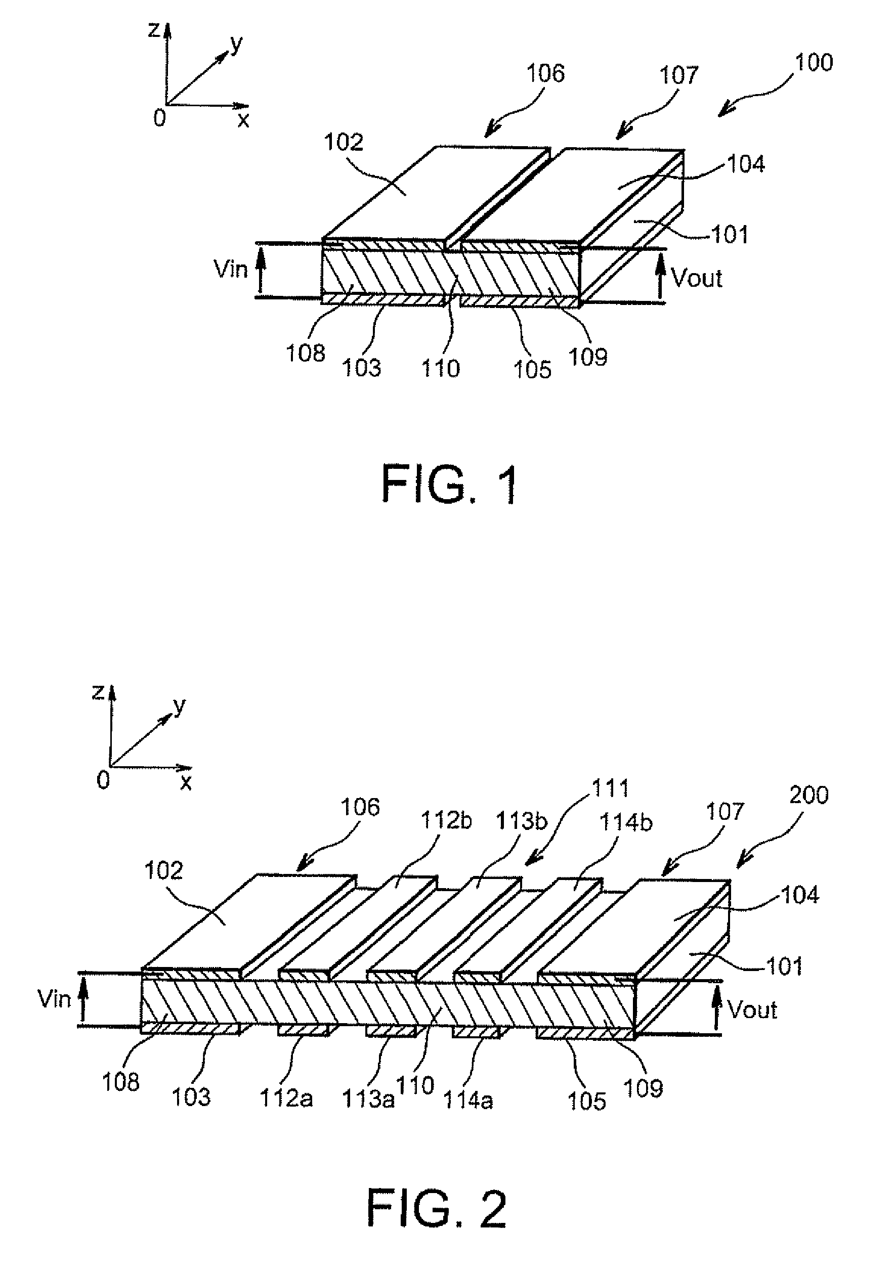
[0046]In this second embodiment, the coupled Lamb wave resonators filter 200 is made to obtain a narrow passband at the output centered around a central frequency equal to about
fc=cλc.
In this case, the length of the layer of resonant material 101 is equal to about
[0047]11λc4.
As in the first embodiment, the length of each resonator 106, 107 is about
[0048]λc2.
Therefore, in this case the length of the portion of resonant material 110 of the periodic lattice 111 is equal to about
[0049]7λc4.
[0050]The periodic lattice 111 comprises a first pair of metal areas 112a, 112b arranged above and below the portion of resonant material 110, and are vertically aligned with each other. These metal areas 112a, 112b are arranged at a distance of about
λc4
from the first resonator 106. A second pair of metal areas 113a, 113b, similar to the first pair of metal areas 112a, 112b, is arranged at a distance of about
λc4
from the first pair of metal areas 112a, 112b. Finally, a third pair of metal areas 114a, 114b
Example
[0072]One example embodiment of this filter 400 according to the fourth embodiment will now be given. A metal deposit is made, for example such as aluminium, platinum, molybdenum and / or tungsten on the two faces of the layer 101 of the resonant material. This may be by PVD deposition. The next step is to etch the metallic deposits, for example by plasma etching, so as to form two electrodes 102, 104 and 103, 105 on each of the faces of the layer 101, the metal areas 112 to 114 to form the period lattice 111, and the metal areas of the Bragg mirrors 115 and 116 as shown in FIG. 4. This embodiment may be implemented by surface micromachining on a substrate or by bulk micromachining.
[0073]In one variation of the fourth embodiment, the portions of the resonant material 117 and 118 of the Bragg mirrors 115 and 116 may comprise alternating parts with high and low acoustic impedances so as to adjust the reflection and dissipation properties of the Bragg mirrors 115 and 116.
[0074]In all four
PUM
| Property | Measurement | Unit |
|---|---|---|
| Time | aaaaa | aaaaa |
| Length | aaaaa | aaaaa |
| Distance | aaaaa | aaaaa |
Abstract
Description
Claims
Application Information
 - R&D Engineer
- R&D Manager
- IP Professional
- Industry Leading Data Capabilities
- Powerful AI technology
- Patent DNA Extraction
Browse by: Latest US Patents, China's latest patents, Technical Efficacy Thesaurus, Application Domain, Technology Topic.
© 2024 PatSnap. All rights reserved.Legal|Privacy policy|Modern Slavery Act Transparency Statement|Sitemap