Packaged device and method of manufacturing the same

Active Publication Date: 2009-01-01
DRNC HLDG INC
View PDF7 Cites 15 Cited by
  • Summary
  • Abstract
  • Description
  • Claims
  • Application Information

AI Technical Summary

Problems solved by technology

A large amount of moisture in the internal space may induce discharging in the vicinity of a driving electrode for the micro movable element.
The induced discharging may degrade the electrical or driving characteristics of the element.
Thus, the use of the moisture absorbent is not preferable for a reduction in package size.
Furthermore, the moisture absorbing effect of the moisture absorbent is likely to be temporally degraded.
This makes it difficult to reliably keep the amount of moisture in the internal space at a low level.

Method used


Image

  • Packaged device and method of manufacturing the same
  • Packaged device and method of manufacturing the same
  • Packaged device and method of manufacturing the same

Examples


Example

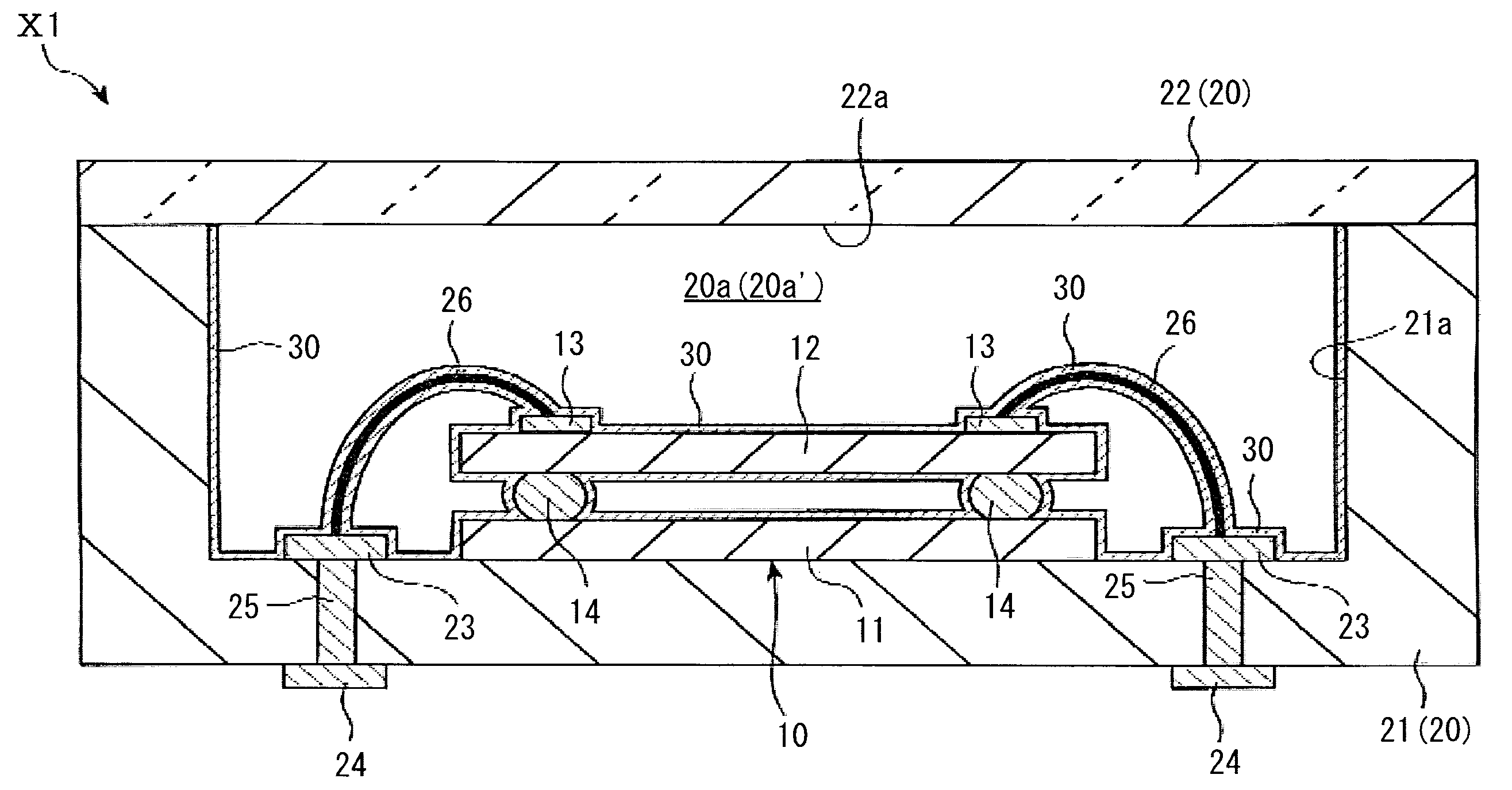
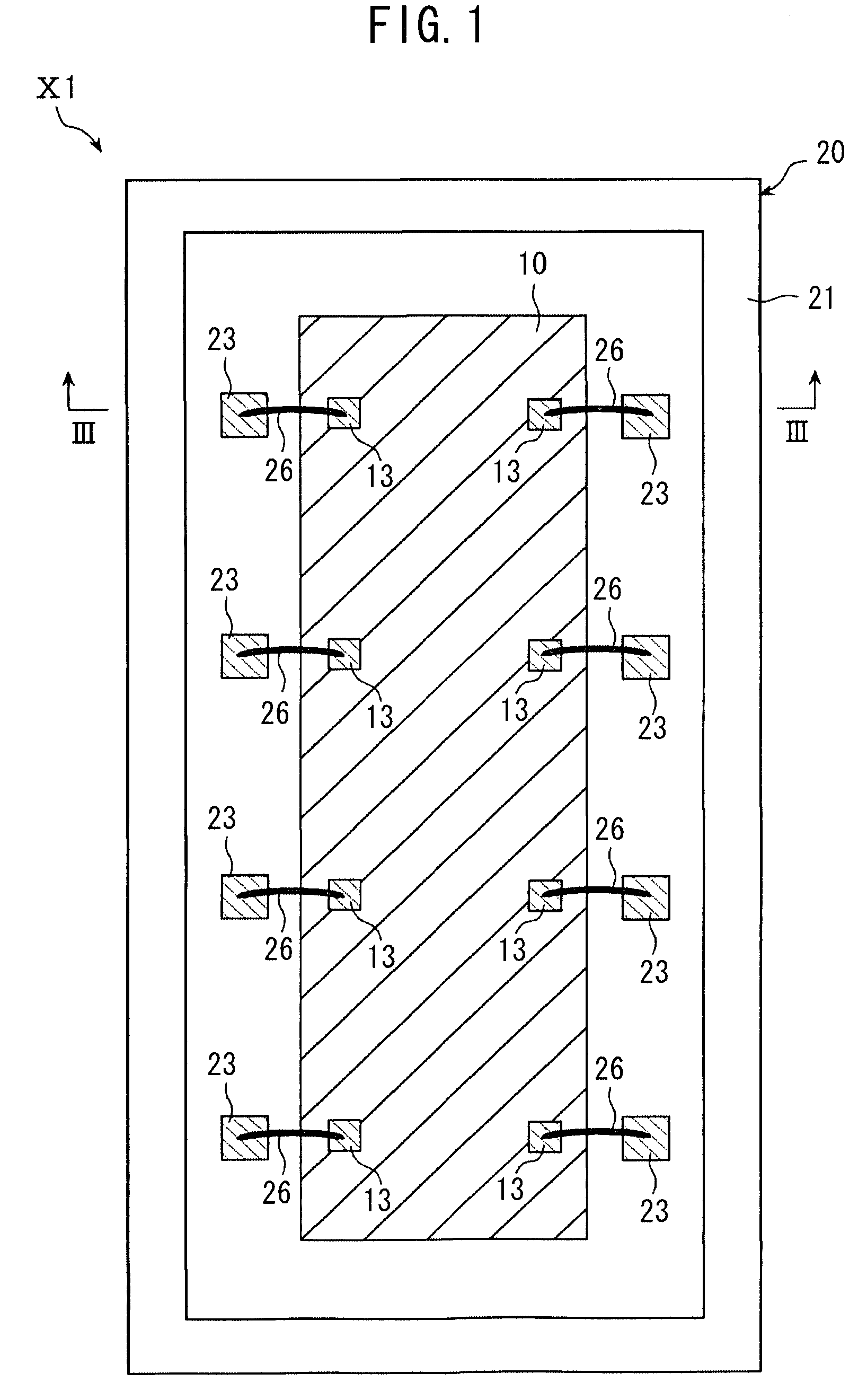
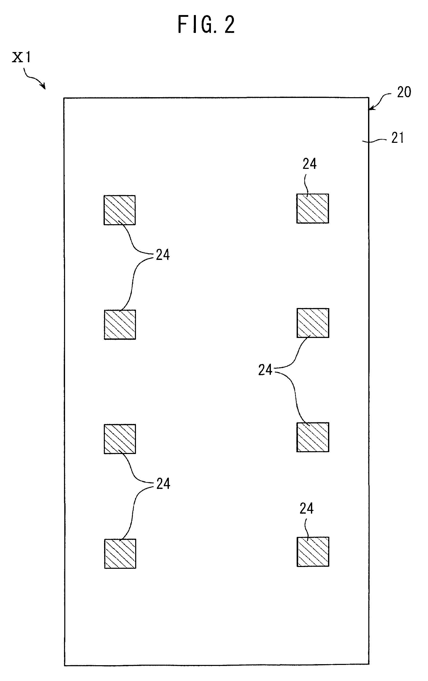
[0029]FIGS. 1 to 3 show a packaged device X1 according to a first aspect of the present embodiment. FIG. 1 is a (partly omitted) plan view of the packaged device X1. FIG. 2 is another plan view of the packaged device X1. FIG. 3 is a sectional view of the packaged device taken along line III-III in FIG. 1.

[0030]The packaged device X1 includes a device chip 10, a package 20, and a parylene film 30 (not shown in FIG. 1).

[0031]In the present aspect, the device chip 10 is what is called a MEMS mirror device. The device chip 10 includes a base substrate 11, a mirror substrate 12, and electrode pads 13. The base substrate 11 and the mirror substrate 12 are joined together via bumps 14. A plurality of micro mirror elements (not shown in FIGS. 1 and 3) are formed in the mirror substrate 12. The plurality of micro mirror elements are formed by processing an SOI (Silicon On Insulator) substrate by a MEMS technique.

[0032]FIG. 4A shows a micro mirror element Y formed in the mirror substrate 12. The


PUM


Abstract

A packaged device includes a package having an inner surface defining a closed internal space, a device chip fixed to the package in the internal space, and a parylene film covering at least a part of the inner surface of the package and/or at least a part of a surface of the device chip.

Description


Claims


Application Information

Patent Timeline
Owner DRNC HLDG INC
Why Eureka
Try Eureka