Semiconductor memory device and method with auxiliary I/O line assist circuit and functionality

a memory device and memory technology, applied in the direction of information storage, static storage, digital storage, etc., can solve the problems of reducing the signal quality of read data from the memory, and the problem of more pronounced problems

Active Publication Date: 2010-02-18
LONGITUDE LICENSING LTD
View PDF6 Cites 2 Cited by
  • Summary
  • Abstract
  • Description
  • Claims
  • Application Information

AI Technical Summary

Benefits of technology

The present invention provides a type of semiconducer that can detect changes caused by external factors like temperature or pressure without affecting its performance significantly. This means it will be more reliable for use with certain types of memories such as dynamic random access memory (RAM).

Problems solved by technology

This patented describes different technical problem addressed in this patents: how efficiently transfers data between memories without sacrificing their performance due to increased electrical stress caused by longer buses needed for faster access times while avoiding interference issues such as cross talk over multiple input/output lines.

Method used


Image

  • Semiconductor memory device and method with auxiliary I/O line assist circuit and functionality
  • Semiconductor memory device and method with auxiliary I/O line assist circuit and functionality
  • Semiconductor memory device and method with auxiliary I/O line assist circuit and functionality

Examples


case # 1

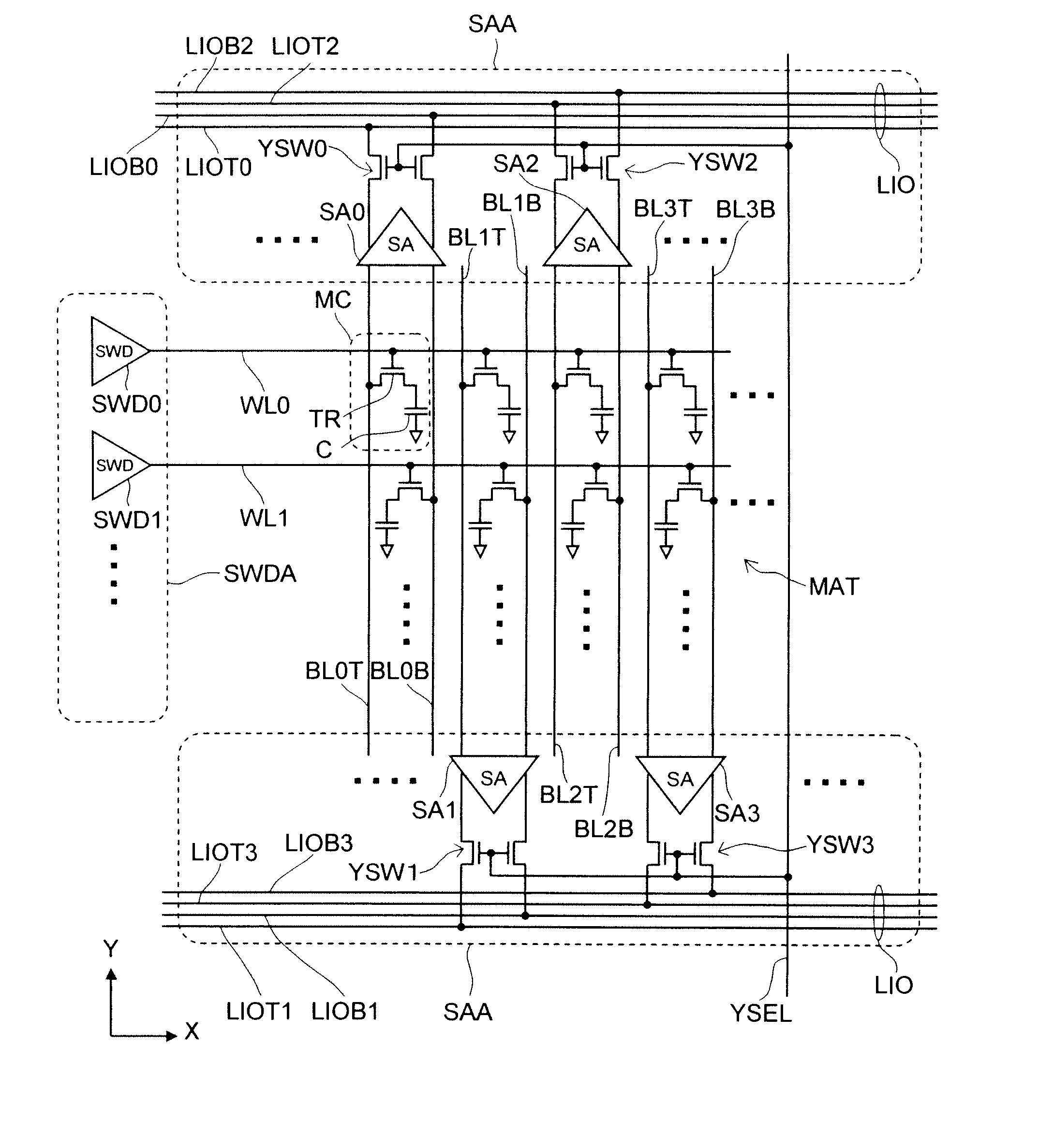
[0065]Case #1 in FIG. 7 is one in which high-level data is written to a memory cell, where the transistor 301 is switched on, and the transistor 302 is switched off. The main I / O line MIO is thereby driven to a high level via the transistor 301. Case #2 is one in which low-level data is written to a memory cell, where the transistor 301 is switched off, and the transistor 302 is switched on. The main I / O line MIO is thereby driven to a low level via the transistor 302. Case #3 is one in which the main I / O line MIO is pre-charged, where the transistor 301 is switched on, and the transistor 302 is switched off. The main I / O line MIO is thereby pre-charged via the transistor 302. Case #4 is one in which a read operation is performed by a read circuit 200, where both the transistors 301 and 302 are switched off. The main I / O line MIO is thereby disconnected from the precharge circuit 300.

[0066]FIG. 8 is a circuit diagram of the assist circuit 400.

[0067]As shown in FIG. 8, the ass


PUM


Abstract

A semiconductor memory device includes an I/O line for transmitting read data that has been read from a memory cell, a plurality of driver circuits for driving the I/O line on the basis of the read data, a read circuit for receiving the read data transmitted through the I/O line, and an assist circuit for amplifying the read data transmitted through the I/O line. The assist circuit is disposed farther away from a prescribed drive circuit included in the plurality of drive circuits as viewed from the read circuit. The signal level can thereby rapidly change levels even in memories having relatively long I/O lines.

Description


Claims


Application Information

Patent Timeline
Owner LONGITUDE LICENSING LTD
Why Eureka
Try Eureka