Amplifier circuit and semiconductor memory device
a technology of amplifier circuit and semiconductor memory device, which is applied in the direction of amplifier with semiconductor device/discharge tube, digital storage, instruments, etc., can solve the problems of not exactly symmetrical design of the pmos and nmos transistor pairs and the bit line sense amplifier /b>10 may not sense and amplify the potential differen
- Summary
- Abstract
- Description
- Claims
- Application Information
AI Technical Summary
Benefits of technology
Problems solved by technology
Method used
Image

Examples
Embodiment Construction
[0025]Exemplary embodiments of the present invention will be described below in more detail with reference to the accompanying drawings. The present invention may, however, be embodied in different forms and should not be construed as limited to the embodiments set forth herein. Rather, these embodiments are provided so that this disclosure will be thorough and complete, and will fully convey the scope of the present invention to those skilled in the art. Throughout the disclosure, like reference numerals refer to like parts throughout the various figures and embodiments of the present invention.
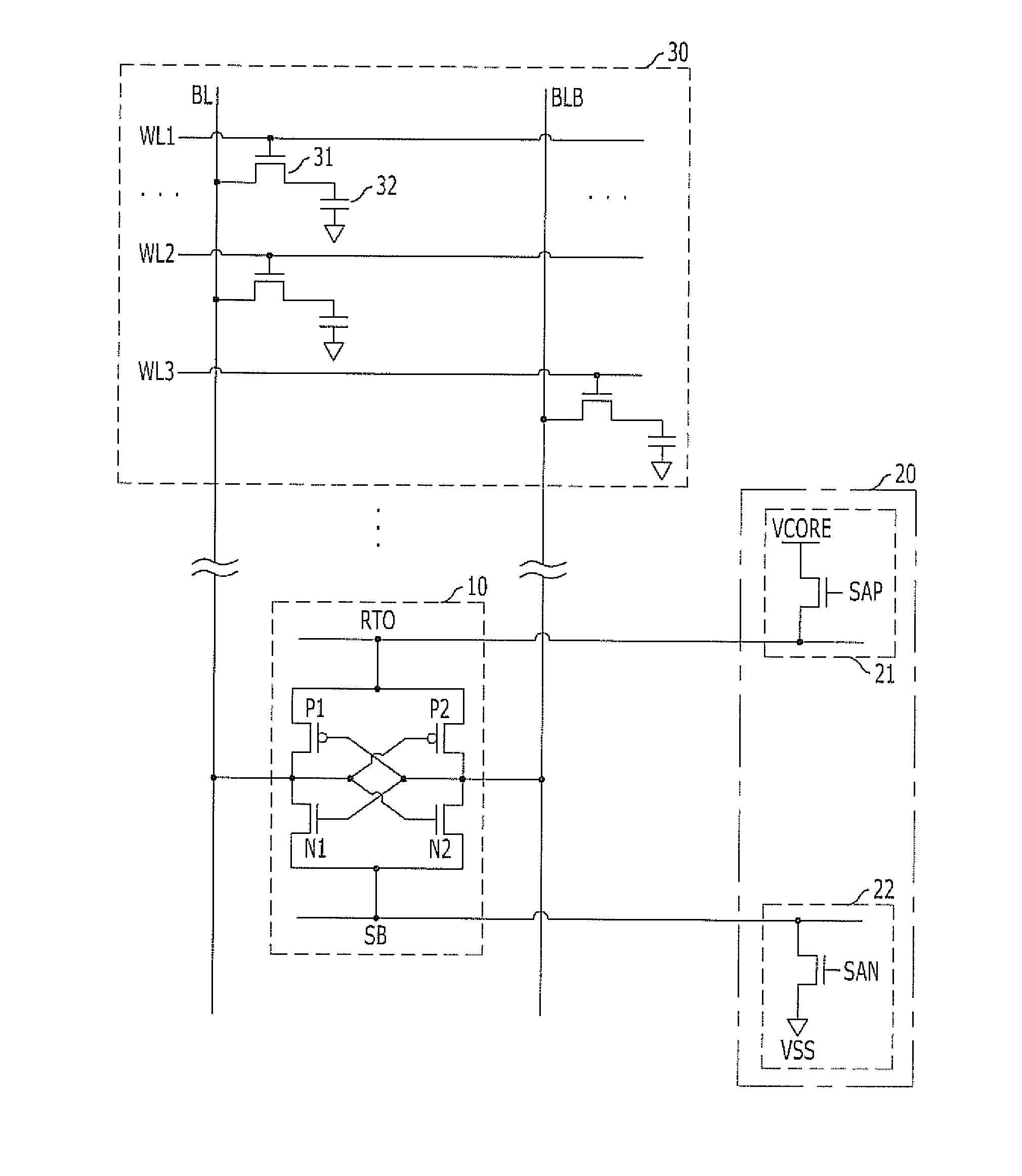
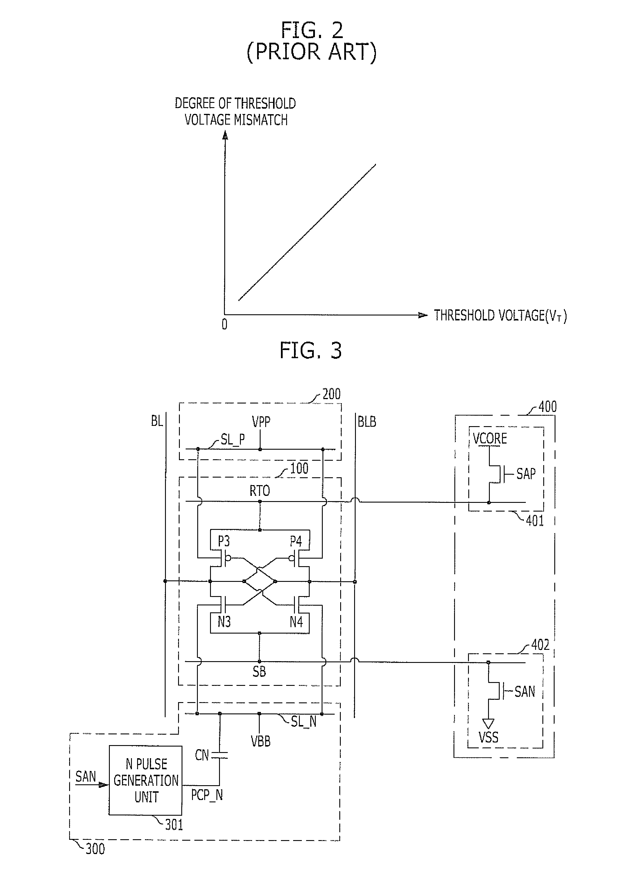
[0026]FIG. 3 is a circuit diagram illustrating a semiconductor memory device in accordance with an embodiment of the present invention.
[0027]The semiconductor memory device may include main / sub bit lines BL and BLB, a sense amplifier 100, a sense amplifier control unit 400, a first back-bias voltage providing unit 200 and a second back-bias voltage providing unit 300.
[0028]The main / sub bit
PUM
 Abstract
Description
Claims
Application Information
 - R&D Engineer
- R&D Manager
- IP Professional
- Industry Leading Data Capabilities
- Powerful AI technology
- Patent DNA Extraction
Browse by: Latest US Patents, China's latest patents, Technical Efficacy Thesaurus, Application Domain, Technology Topic.
© 2024 PatSnap. All rights reserved.Legal|Privacy policy|Modern Slavery Act Transparency Statement|Sitemap