Semiconductor device and semiconductor device manufacturing method
- Summary
- Abstract
- Description
- Claims
- Application Information
AI Technical Summary
Benefits of technology
Problems solved by technology
Method used
Image

Examples
first embodiment
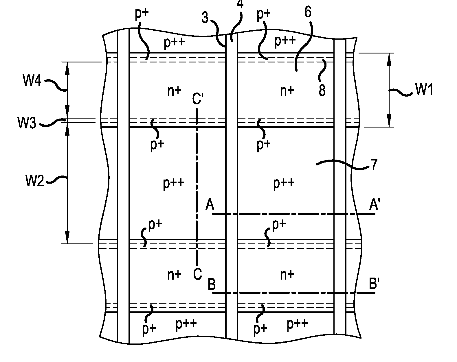
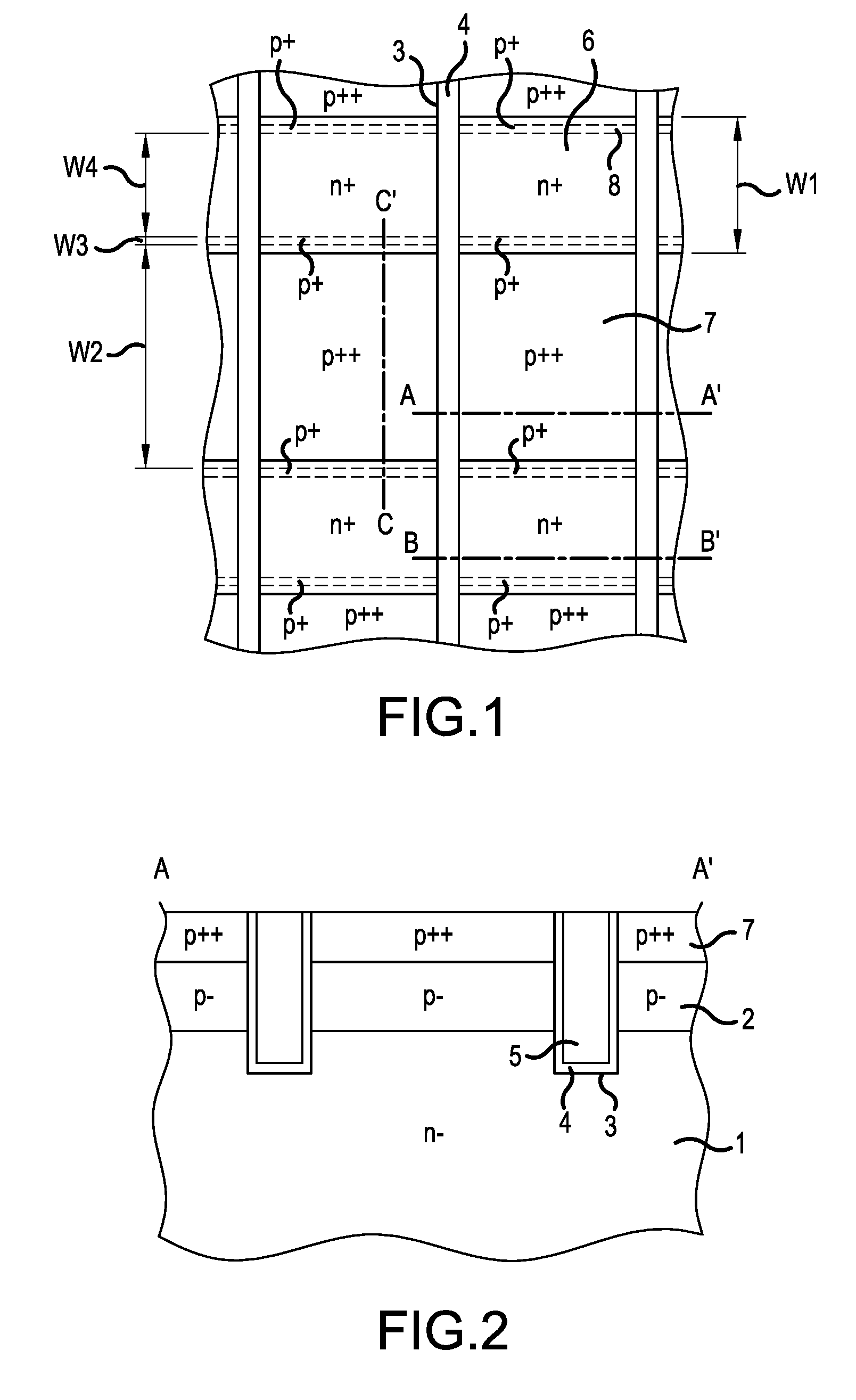
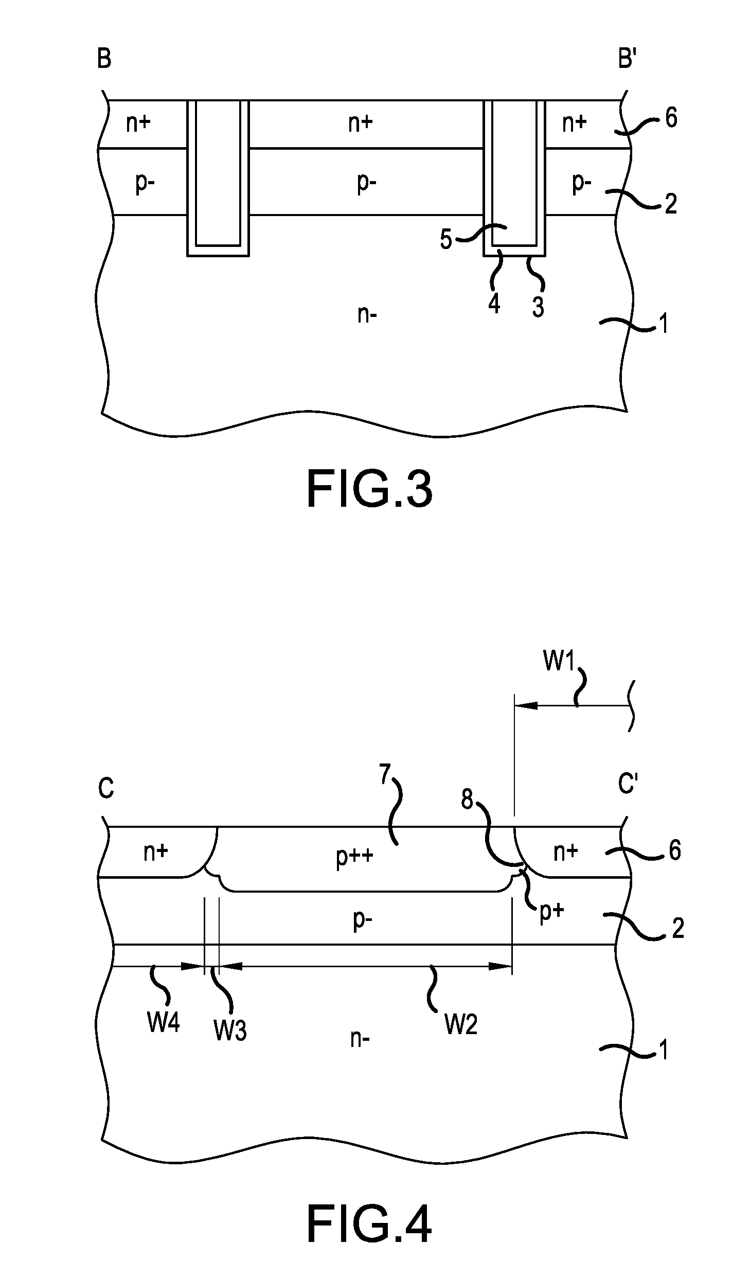
[0056]A description will be given of the structure of a semiconductor device according to a first embodiment. FIG. 1 is a plan view showing the planar layout of a trench gate structure of the semiconductor device according to the first embodiment. A gate dielectric, interlayer dielectric, source electrode, and passivation film are omitted from FIG. 1 (the same applies to FIGS. 2 to 4, 10, and 14). FIG. 2 is a sectional view showing the sectional structure along a section line A-A′ of FIG. 1. FIG. 3 is a sectional view showing the sectional structure along a section line B-B′ of FIG. 1. FIG. 4 is a sectional view showing the sectional structure along a section line C-C′ of FIG. 1. The section line A-A′ passes through a trench 3 and a p++-type contact region (fourth semiconductor region) 7. The section line B-B′ passes through the trench 3 and an n+-type emitter region (third semiconductor region) 6. The section line C-C′ passes through the n+-type emitter region 6, the p++-type contact
second embodiment
[0082]A description will be given of the structure of a semiconductor device according to a second embodiment. FIG. 10 is a sectional view showing main portions of a trench gate structure of the semiconductor device according to the second embodiment. FIG. 10 shows the sectional structure along the section line C-C′ of FIG. 1. The planar layout of the trench gate structure, the sectional structure passing through the trench 3 and p++-type contact region 7 (the section line A-A′ of FIG. 1), and the sectional structure passing through the trench 3 and n+-type emitter region 6 (the section line B-B′ of FIG. 1) are the same as in the first embodiment (refer to FIGS. 1 to 3). The semiconductor device according to the second embodiment differs from the semiconductor device according to the first embodiment in that the depth of a p+-type region 28 that covers an end portion on the lower side of the junction interface between the n+-type emitter region 6 and p++-type contact region 7 is greate
third embodiment
[0089]A description will be given of the structure of a semiconductor device according to a third embodiment. FIG. 14 is a perspective view showing main portions of a trench gate structure of the semiconductor device according to the third embodiment. The semiconductor device according to the third embodiment differs from the semiconductor device according to the first embodiment in that a mesa portion configured as a unit cell structure by providing the n+-type emitter region 6, and a mesa portion configured as a p−-type floating region 42 without providing the n+-type emitter region 6, are disposed in the p−-type base region 2 sandwiched by neighboring trenches 3. Specifically, a mesa portion configured as a unit cell formed of the n+-type emitter region 6 and p++-type contact region 7 and a mesa portion configured as the p−-type floating region 42, which has emitter potential, are repeatedly alternately disposed in the second direction perpendicular to the first direction, in which
PUM
 Abstract
Description
Claims
Application Information
 - R&D Engineer
- R&D Manager
- IP Professional
- Industry Leading Data Capabilities
- Powerful AI technology
- Patent DNA Extraction
Browse by: Latest US Patents, China's latest patents, Technical Efficacy Thesaurus, Application Domain, Technology Topic.
© 2024 PatSnap. All rights reserved.Legal|Privacy policy|Modern Slavery Act Transparency Statement|Sitemap