Semiconductor module

a technology of semiconductor modules and semiconductor modules, applied in the direction of dc-ac conversion without reversal, semiconductor/solid-state device details, pulse techniques, etc., can solve the problems of increasing the number of input/output terminals of semiconductor modules, requiring time, and inevitably taking time for operation status information to be output, so as to facilitate detection and consolidate the function of abnormality countermeasures. simple and efficient

Active Publication Date: 2015-12-24
FUJI ELECTRIC CO LTD
View PDF4 Cites 2 Cited by
  • Summary
  • Abstract
  • Description
  • Claims
  • Application Information

AI Technical Summary

Benefits of technology

The inventors have developed a new type of semiconducer called the SemiWafer Module (SIM). This allows multiple signals to operate at once within its own housing while also being able to receive operating condition data outside through their leads attached to them. By connecting these outputs together they provide more flexibility than traditional systems where there were only two connections between controllers and sensing devices. Additionally, SIM modules allow for quicker detection of any issues during manufacturing processes due to fewer inputs and outcomes compared to previous methods like separate connectivity arrangements. Overall, the technical effect of this innovation lies in improving efficiency and reliability in electronic components used in industrial applications.

Problems solved by technology

This patented describes a system called a Semi-conducer Module Imaging Device (SIMD). It uses multiple switches arranged together along one axis to create a circuit path through which electrical energy can flow from one side to another. Each switch includes two transistors - either alone or combined into groups – forming part of its own design. By controlling signals at both ends of certain ones of those transistor pairs, it becomes possible to monitor whether there're any faulty connections within specific parts of the circuit. Additionally, the components inside the circuit include input capacitors and drain currents, providing protection against excessive voltages during normal use conditions. Overall, the technical problem addressed by this patent relates to improving the performance and reliability of electronic devices utilizing semiconctor modules

Method used


Image

  • Semiconductor module
  • Semiconductor module
  • Semiconductor module

Examples


Embodiment Construction

[0023]Below, a semiconductor module relating to one embodiment of the present invention is described below with reference to the drawings.

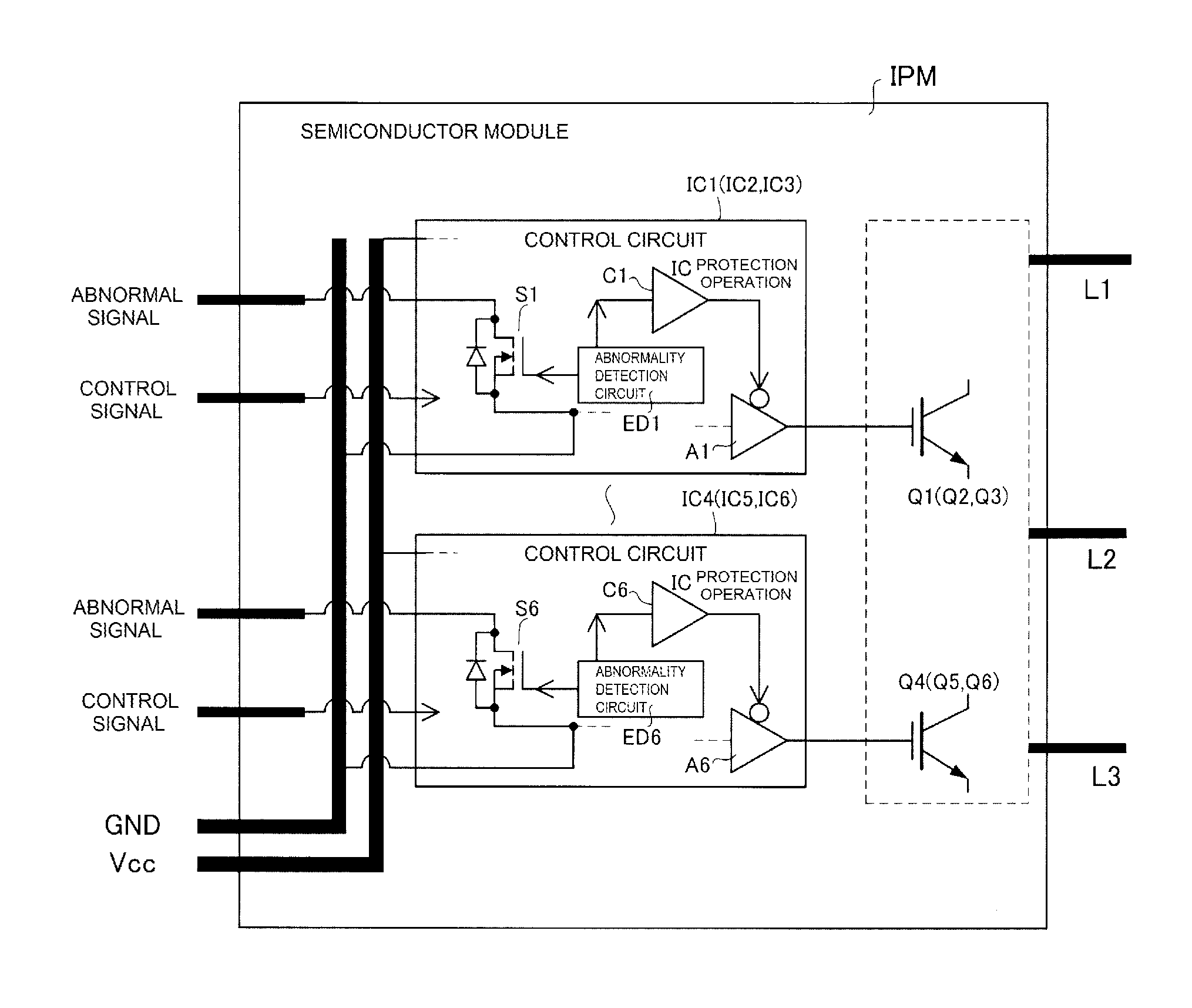
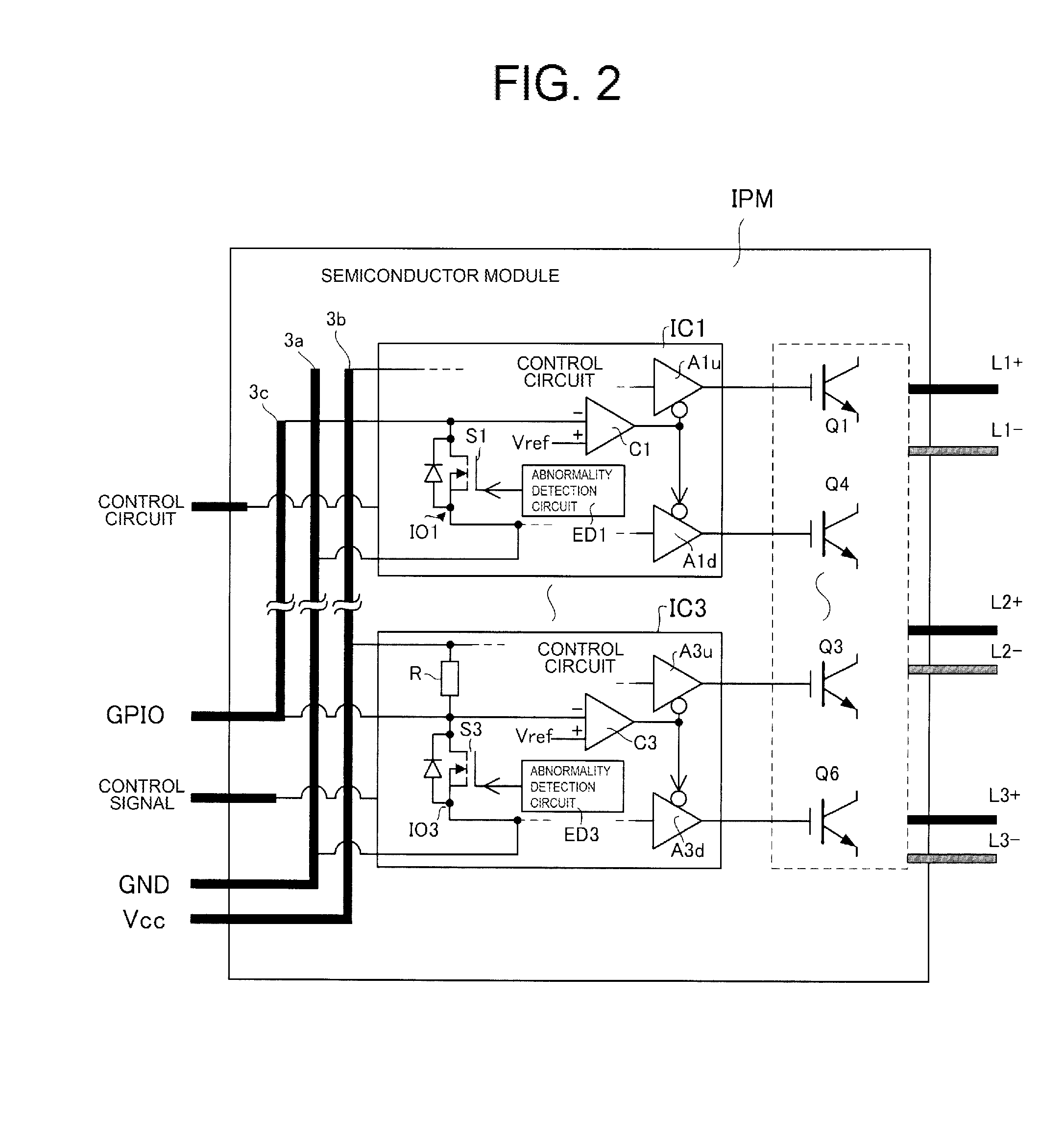
[0024]FIG. 1 is a general schematic drawing of the semiconductor module IPM relating to the present invention. The semiconductor module IPM shown in FIG. 1 is provided with six switching elements Q1, Q2 to Q6 and six free-wheeling diodes D1, D2 to D6 which form three half-bridge circuits. Furthermore, the semiconductor module IPM is constituted by three control circuits IC1, IC2, IC3 which drive the switching elements Q1, Q2 to Q6 on and off respectively in complementary fashion, for each of the half-bridge circuits. Here, a semiconductor module IPM which forms three half-bridge circuits is described, but it is also possible to form two or four or more half-bridge circuits.

[0025]Incidentally, the six switching elements Q1, Q2 to Q6 are constituted by IGBTs, for example, and basically, are connected in series in pairs of two elements each, so as to fo


PUM


Abstract

A semiconductor module which includes a plurality of control circuits that respectively drive a plurality of semiconductor elements on and off and a plurality of signal output circuits for the respective control circuits and which output operation status information, where the signal output circuits are respectively provided with signal output terminals having an open-drain configuration, and the signal output terminals each are connected to an internal lead frame on which the power semiconductor elements and the control circuits are mounted.

Description


Claims


Application Information

Patent Timeline
Owner FUJI ELECTRIC CO LTD
Why Eureka
Try Eureka