Display device and operation method thereof
a display device and display technology, applied in the field of display devices, can solve the problems of noise influence and degradation of the detection sensitivity of the touch sensor unit, and achieve the effects of smooth input, high detection sensitivity, and high detection sensitivity
- Summary
- Abstract
- Description
- Claims
- Application Information
AI Technical Summary
Benefits of technology
Problems solved by technology
Method used
Image

Examples
embodiment 1
[0076]In this embodiment, a display device including a display unit and a touch sensor unit is described. In particular, the relation between image rewriting operation by the display unit and detection operation by the touch sensor unit is described.
>
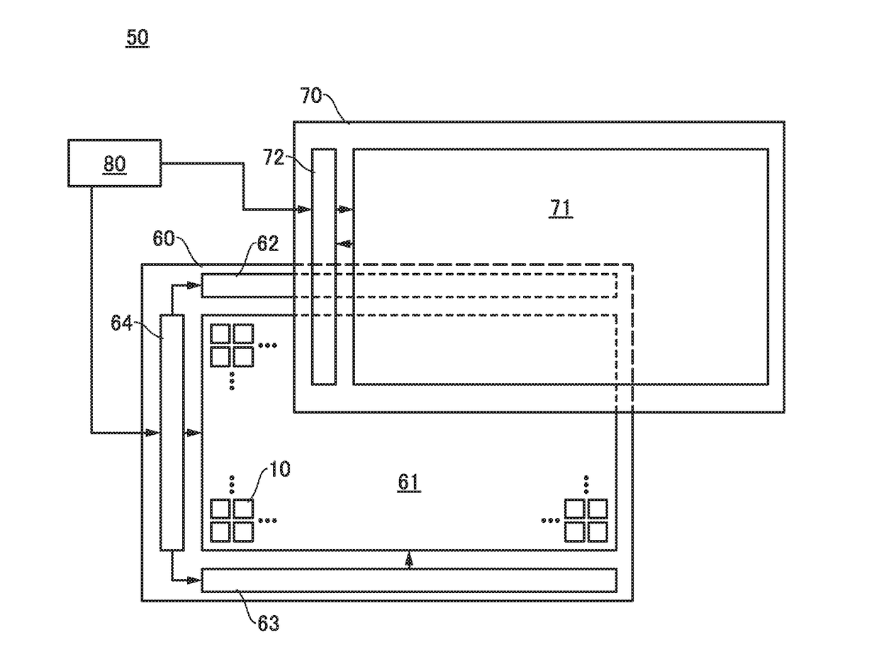
[0077]FIG. 1 is a block diagram illustrating a structure example of a display device. A display device 50 includes a display unit 60, a touch sensor unit 70, and an application processor 80.
[0078]The display unit 60 includes a pixel array 61, a gate driver 62, a gate driver 63, and a source driver IC 64.
[0079]The pixel array 61 includes a plurality of pixels 10, and each pixel 10 is an active element driven by a transistor. The pixel array 61 has a function of forming a display region of the display unit 60 and displaying an image. A more specific structure example of the pixel array 61 is described in Embodiments 4 to 6.
[0080]The gate driver 62 and the gate driver 63 have a function of driving a gate line for selecting the pixel 10. Only
embodiment 2
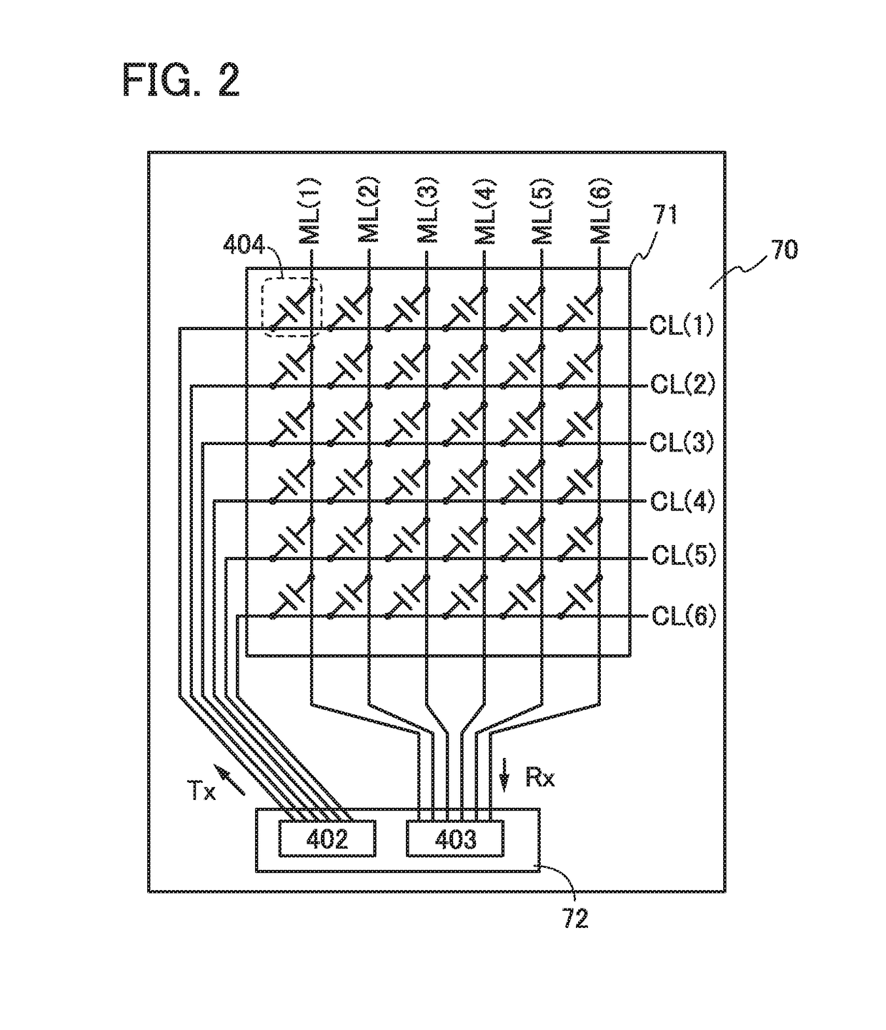
[0158]In this embodiment, a structure example of the touch sensor unit 70 mentioned in the above embodiment is described with reference to FIGS. 16A to 16C and FIGS. 17A and 17B.
[0159]A specific structure example of the touch sensor unit 70 is described with reference to FIGS. 16A to 16C and FIGS. 17A and 17B.
[0160]FIG. 16A is a top view of the touch sensor unit 70. FIGS. 16B and 16C are each a projection view illustrating part of FIG. 16A.
[0161]FIG. 17A is a top view of a portion in which a control line and a sensing signal line are adjacent to each other. FIG. 17B is a projection view that schematically illustrates an electric field generated in the adjoining portion.
[0162]The touch sensor unit 70 includes the sensor array 71. The sensor array 71 includes a wiring CL(g), a wiring ML(h), and a conductive film (see FIG. 16A). Note that g and h are each an integer of 2 or more.
[0163]For example, a conductive film divided into a plurality of regions can be used for the sensor array 71 (s
embodiment 3
[0178]In this embodiment, a structure example of the source driver IC 64 mentioned in the above embodiment is described with reference to FIGS. 40A and 40B.
[0179]FIGS. 40A and 40B are block diagrams of the source driver IC 64 in the case where a hybrid element including a reflective element and a light-emitting element is used for the pixel 10.
[0180]The source driver IC 64 illustrated in FIG. 40A includes a control circuit 801, a driver 802, a frame memory 803, a frame memory 804, a gate driver signal generation circuit 806, and a gate driver signal generation circuit 807.
[0181]The control circuit 801 has a function of receiving a signal from the application processor 80 and transmitting the signal to each circuit included in the source driver IC 64. Examples of interface standards of the signal transmitted from the application processor 80 to the control circuit 801 include a mobile industry processor interface (MIPI) and a serial peripheral interface (SPI).
[0182]The driver 802 has a
PUM
 Abstract
Description
Claims
Application Information
 - R&D Engineer
- R&D Manager
- IP Professional
- Industry Leading Data Capabilities
- Powerful AI technology
- Patent DNA Extraction
Browse by: Latest US Patents, China's latest patents, Technical Efficacy Thesaurus, Application Domain, Technology Topic.
© 2024 PatSnap. All rights reserved.Legal|Privacy policy|Modern Slavery Act Transparency Statement|Sitemap