Laser module
a laser module and laser technology, applied in the direction of semiconductor laser structure details, semiconductor amplifier structure, semiconductor lasers, etc., can solve problems such as inability to control
- Summary
- Abstract
- Description
- Claims
- Application Information
AI Technical Summary
Benefits of technology
Problems solved by technology
Method used
Image

Examples
first embodiment
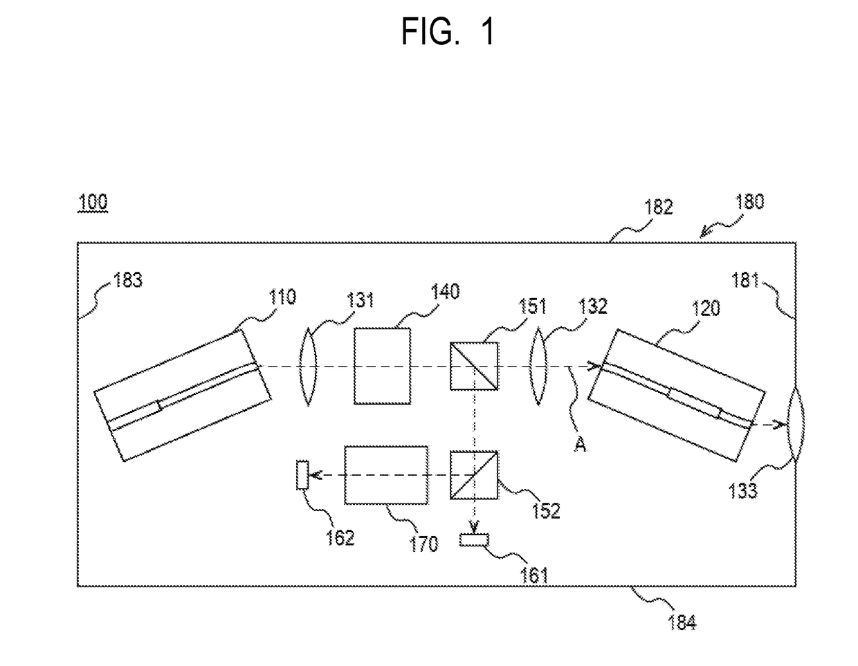
[0027]FIG. 1 is a general configuration diagram of a laser module 100 according to the present embodiment. The laser module 100 has a laser element 110, an optical amplifier 120, a collimate lens 131, condensing lenses 132 and 133, an optical isolator 140, optical splitters 151 and 152, photodiodes 161 and 162, and an etalon filter 170 within a casing 180 (package). Each member within the laser module 100 is connected to a not-shown control unit, and power supply and behavior control of the laser module 100 are performed by the control unit.
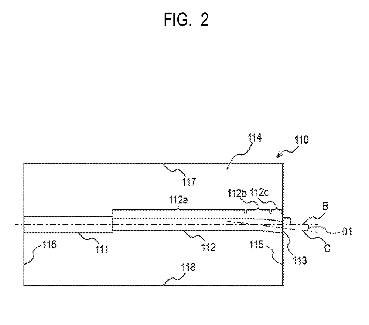
[0028]The laser element 110 generates and outputs a laser light A. The detailed configuration of the laser element 110 will be described later by using FIG. 2.
[0029]The collimate lens 131 is provided in a direction in which the laser element 110 outputs the laser light A and converts the laser light A output from the laser element 110 into a parallel light. The optical isolator 140 is provided in a direction in which the collimate lens 131 outputs t
second embodiment
[0065]FIG. 8 is a general configuration diagram of a laser module 200 according to the present embodiment. While the laser module 200 has the same components as the laser module 100 of the first embodiment, the arrangement of the optical amplifier 120 is different. Specifically, unlike the first embodiment, the optical amplifier 120 is inverted along the short direction of the casing 180.
[0066]FIG. 9 is a schematic diagram illustrating an arrangement of the laser element 110 and the optical amplifier 120 in the present embodiment. The laser element 110 and the optical amplifier 120 are arranged nonparallel relative to each other such that the laser light A output from the output port 113 of the laser element 110 is input to the input port 123 of the optical amplifier 120. Unlike the first embodiment, the laser element 110 and the optical amplifier 120 are not arranged at an angle that is not linear or parallel but arranged in substantially the same direction. The laser light A is emitt
third embodiment
[0068]FIG. 10 is a general configuration diagram of a laser module 300 according to the present embodiment. The laser module 300 is different from that of the first embodiment in that the optical waveguide 122 does not have the curved part 122b and is formed of only the first linear part 122a between the first end face (input end face) 125 side on which the input port 123 is provided and the optical amplifier unit 121. Further, because of this, the laser module 300 is partially different from that of the first embodiment in the arrangement and configuration of elements.
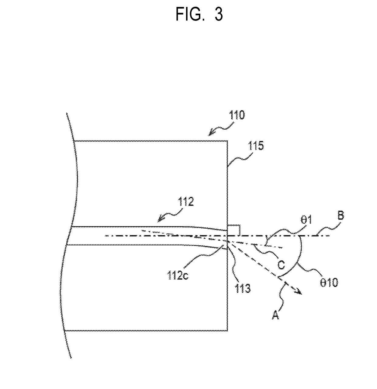
[0069]While, in the first and second embodiments, the case where the optical waveguide 112 is nonparallel relative to the output end face 115 in the laser element 110 and connected thereto and the optical waveguide 122 is nonparallel relative to the input end face 125 in the optical amplifier 120 and connected thereto has been described, the invention is not limited thereto. It may be sufficient that at least the optical
PUM
 Abstract
Description
Claims
Application Information
 - R&D Engineer
- R&D Manager
- IP Professional
- Industry Leading Data Capabilities
- Powerful AI technology
- Patent DNA Extraction
Browse by: Latest US Patents, China's latest patents, Technical Efficacy Thesaurus, Application Domain, Technology Topic.
© 2024 PatSnap. All rights reserved.Legal|Privacy policy|Modern Slavery Act Transparency Statement|Sitemap