Semiconductor device packaged in plastic package
a technology of semiconductor devices and plastic packages, which is applied in the direction of semiconductor devices, semiconductor/solid-state device details, electrical apparatus, etc., can solve the problems of difficult stress absorption of lead 603 and mechanical and electric connection between end 603a and foot prin
- Summary
- Abstract
- Description
- Claims
- Application Information
AI Technical Summary
Benefits of technology
Problems solved by technology
Method used
Image

Examples
first embodiment
A semiconductor device packaged in a plastic package provided with J-shaped leads.
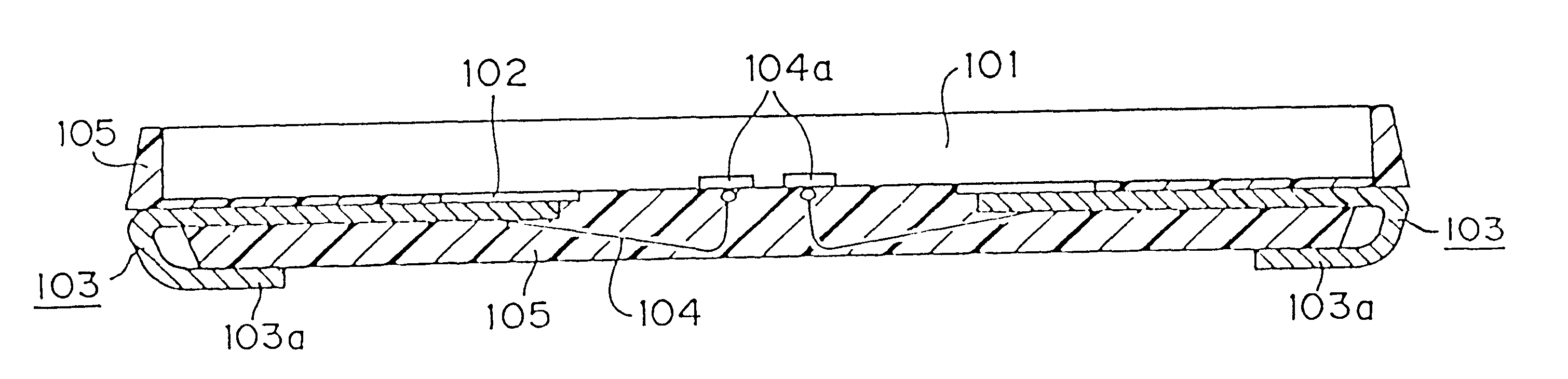
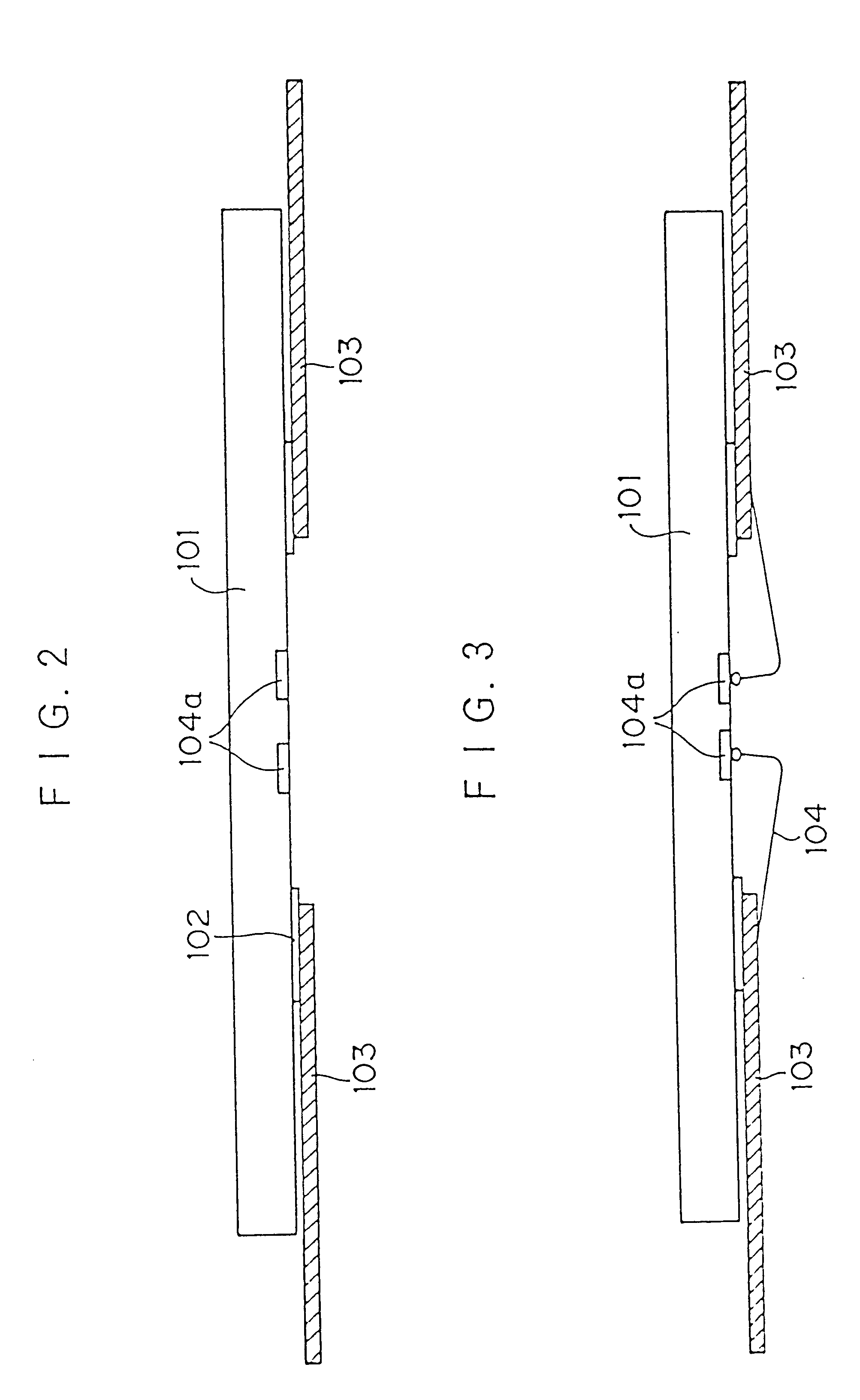
Referring to FIG. 2, each of plural leads made of an alloy containing 42% Ni and 58% Fe and having the coefficient of linear expansion of 4.times.10.sup.-6 / .degree. C. 103 is adhered to the top surface (the rear surface in the drawings) of a semiconductor device chip of which the dimension is 15 mm in length, 6 mm in width and 0.3 mm in thickness 101 by employing an adhesive tape e.g. a polyimide tape 102. The leads 103 are arranged in parallel to one another. The length of the leads 103 is long enough to allow to be bent. The coefficient of linear expansion is 3.times.10.sup.-6 / .degree. C. for an Si substrate of the semiconductor device chip 101 and is 10.times.10.sup.-6 / .degree. C. for epoxy resin.
Referring to FIG. 3, each of the leads 103 is bonded with each of bonding pads 104a produced on the top surface of the semiconductor device chip 101, by an Au wire 104.
Referring to FIG. 4, a molding p
second embodiment
A semiconductor device packaged in a plastic package provided with U-shaped leads, the U-shaped leads being arranged remote form the edge of the semiconductor device.
Referring to FIG. 7, each of plural leads 303 is adhered to the top surface (the bottom surface in the drawings) of a semiconductor device chip 301 by employing an adhesive tape e.g. a polyimide tape 302. The length of the lead 303 is much shorter than that of the first embodiment. Each of the leads 303 is bonded with each of bonding pads 304a produced on the top surface of the semiconductor device chip 301, by employing an Au wire 304.
Referring to FIG. 8, a molding process is conducted to cover the central area of the top surface of and the side surface of the semiconductor device chip 301. Epoxy resin is employed for the plastic mold. Attention is paid to make the thickness of a plastic mold 305 produced along the side of the semiconductor device chip 301 thin e.g. 0.3 through 0.4 mm for the purpose to make the horizonta
third embodiment
A semiconductor device packaged in a plastic package, the location of the package being limited to the central area of the top surface of a semiconductor device chip, and the semiconductor device being provided with J-shaped leads whose top surface is not higher than the top surface of the package.
Referring to FIG. 11, each of plural leads 503 is adhered to the top surface (the rear surface in the drawings) of a semiconductor device chip 501 by employing an adhesive tape e.g. a polyimide tape 502. The length of the lead 503 is long. In other words, the length of the lead 503 is approximately same as that of the first embodiment. Each of the leads 503 is bonded with each of bonding pads 504a produced on the top surface of the semiconductor device chip 501, by employing an Au wire 504.
Referring to FIG. 12, a molding process is conducted to cover the central area of the top surface of and the side surface of the semiconductor device chip 501. The thickness of the plastic mold 505 produced
PUM
 Abstract
Description
Claims
Application Information
 - R&D Engineer
- R&D Manager
- IP Professional
- Industry Leading Data Capabilities
- Powerful AI technology
- Patent DNA Extraction
Browse by: Latest US Patents, China's latest patents, Technical Efficacy Thesaurus, Application Domain, Technology Topic.
© 2024 PatSnap. All rights reserved.Legal|Privacy policy|Modern Slavery Act Transparency Statement|Sitemap