Method and apparatus for indicating directionality in integrated circuit manufacturing
An integrated circuit, directional technology, applied in the direction of circuits, semiconductor/solid-state device manufacturing, electrical components, etc.
- Summary
- Abstract
- Description
- Claims
- Application Information
AI Technical Summary
Problems solved by technology
Method used
Image

Examples
Embodiment Construction
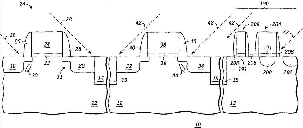
[0018] figure 1 A cross-sectional view of an integrated circuit 10 is shown that includes an indicator 190 in accordance with one embodiment of the present invention. Integrated circuit 10 includes device 14 with implant direction A and device 16 with implant direction B and indicator 190 , all formed on semiconductor substrate 12 . In one embodiment, implantation direction A may have a first implantation direction and implantation direction B may have a second implantation direction. The semiconductor substrate 12 may be any semiconductor material or combination of materials, such as gallium arsenide, silicon germanium, silicon-on-insulator (SOI) (eg, fully depleted SOI (FDSOI)), silicon, monocrystalline silicon, etc., and combinations thereof .
[0019] In one embodiment, device 14 is an NMOS device and device 16 is a PMOS device, or vice versa. In another embodiment, devices 14 and 16 may both be NMOS or both PMOS, with different asymmetric implant directions. Device 14 in
PUM
 Abstract
Description
Claims
Application Information
 - R&D Engineer
- R&D Manager
- IP Professional
- Industry Leading Data Capabilities
- Powerful AI technology
- Patent DNA Extraction
Browse by: Latest US Patents, China's latest patents, Technical Efficacy Thesaurus, Application Domain, Technology Topic.
© 2024 PatSnap. All rights reserved.Legal|Privacy policy|Modern Slavery Act Transparency Statement|Sitemap