Manufacturing method of circuit module
A circuit module and process technology, applied in circuits, semiconductor/solid-state device manufacturing, electrical components, etc., can solve the problems of rising circuit module manufacturing costs, large amount of resin, and difficulty in thinning circuit modules, so as to reduce manufacturing costs. Effect
- Summary
- Abstract
- Description
- Claims
- Application Information
AI Technical Summary
Problems solved by technology
Method used
Image

Examples
no. 1 approach
[0051] Configuration of the circuit module related to the first embodiment of the present invention
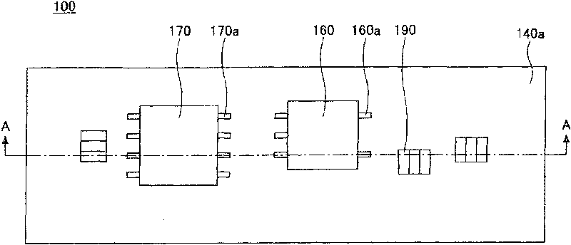
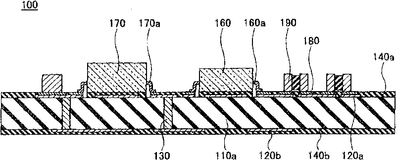
[0052] First, the structure of the circuit module according to the first embodiment of the present invention will be described. Figure 7 It is a plan view illustrating the circuit module according to the first embodiment of the present invention. Figure 8 is along Figure 7 Sectional view of line C-C. refer to Figure 7 as well as Figure 8 , the circuit module 10 has a substrate 11a, wiring patterns 12a and 12b, through holes 13, solder protection layers 14a and 14b, adhesive 15, FET bare chip 16, bonding wire 16a, IC bare chip 17, bonding wire 17a, paste Solder material 18 , electronic component 19 , and sealing resin 20 .
[0053] In the circuit module 10, a wiring pattern 12a is formed on one surface of the substrate 11a, and a portion (hereinafter referred to as "pad") having an opening is formed on the wiring pattern 12a to be electrically connected to a mounted comp
Embodiment approach
[0077] According to the first embodiment of the present invention, by sealing only bare chips such as FETs and ICs with a sealing resin, compared with conventional circuit modules in which not only bare chips such as FETs and ICs are sealed but also electronic components, the cost can be reduced. The use amount of the materials constituting the sealing resin can suppress the increase of the manufacturing cost. In addition, by sealing only bare chips such as FETs and ICs with a sealing resin, even when electronic components are thicker than bare chips such as FETs and ICs, the overall thickness of the circuit module can be reduced (low profile) . Furthermore, since the area of the sealing resin in the portion in contact with the substrate is smaller than that of a conventional circuit module, warping of the substrate can be reduced.
[0078] Furthermore, according to the first embodiment of the present invention, since the circuit module is manufactured in the order of the bare
no. 2 approach
[0082] Configuration of the circuit module related to the second embodiment of the present invention
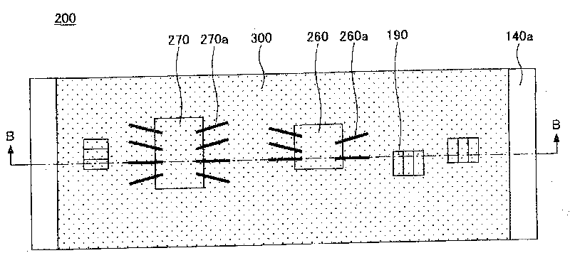
[0083] First, the structure of the circuit module according to the second embodiment of the present invention will be described. Figure 17 It is a plan view illustrating the circuit module according to the second embodiment of the present invention. Figure 18 is along Figure 17 Sectional view of E-E line. exist Figure 17 as well as Figure 18 In, about with Figure 7 as well as Figure 8 The same symbols are attached to the same parts, and descriptions thereof may be omitted. refer to Figure 17 as well as Figure 18 , the circuit module 30 will Figure 7 as well as Figure 8 The FET bare chip 16 and IC bare chip 17 of the illustrated circuit module 10 are replaced with FET36 and IC37 of the CSP package, and the bonding wires 16a and 17a are replaced with terminals 36a and 37a. Other parts of the circuit module 30 are configured in the same manner as the circuit m
PUM
| Property | Measurement | Unit |
|---|---|---|
| Thickness | aaaaa | aaaaa |
| Thickness | aaaaa | aaaaa |
Abstract
Description
Claims
Application Information
 - R&D Engineer
- R&D Manager
- IP Professional
- Industry Leading Data Capabilities
- Powerful AI technology
- Patent DNA Extraction
Browse by: Latest US Patents, China's latest patents, Technical Efficacy Thesaurus, Application Domain, Technology Topic.
© 2024 PatSnap. All rights reserved.Legal|Privacy policy|Modern Slavery Act Transparency Statement|Sitemap