Meta-material absorber based on dendritic structure
A technology of metamaterials and absorbers, applied in electrical components, magnetic field/electric field shielding, etc., can solve problems such as large metal ohmic loss and dielectric loss
- Summary
- Abstract
- Description
- Claims
- Application Information
AI Technical Summary
Problems solved by technology
Method used
Image

Examples
Embodiment 1
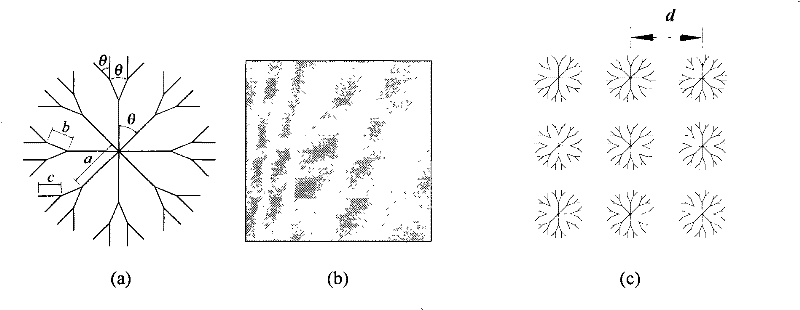
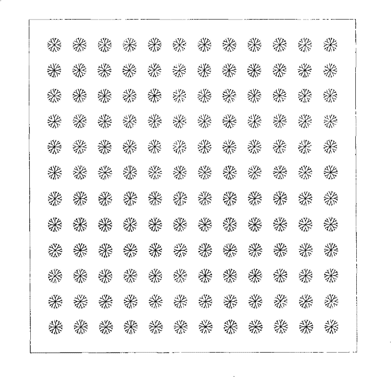
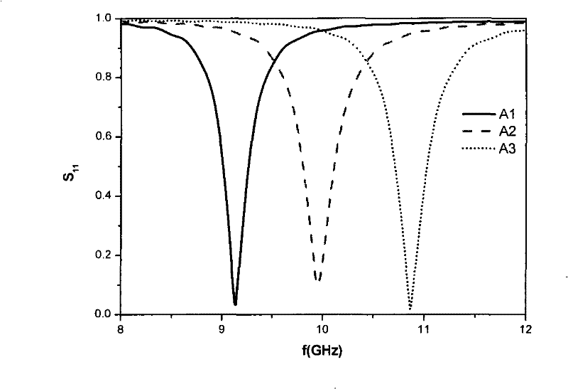
[0013] Using circuit board etching technology, the metal dendritic structure unit array is etched on one side of the epoxy phenolic glass fiber PCB substrate with a thickness of 0.8mm, and the other side is a metal film. The tertiary branch lengths of the metal branches are a=1.2mm, b=0.9mm, c=0.8mm respectively, and the unit lattice spacing is d=10.0mm. Cut the etched PCB board into a size of 130mm×130mm to complete the fabrication of the invented metamaterial absorber A-1. S of Metamaterial Absorber A-1 11 , S 21 curve like image 3 , as shown in 4. It can be seen from the figure that around 9.13GHz, S 11 A minimum value of 0.035 is reached, S 21 The curve is always equal to 0. The absorption rate can be expressed as A(ω)=1-|S 11 | 2 -|S 21 | 2 . from Figure 5 It can be seen from the absorption curve that the absorption rate reaches 99.88% at 9.13GHz.
Embodiment 2
[0015] Using circuit board etching technology, a metal dendritic structure unit array is etched on one side of the epoxy phenolic glass fiber PCB substrate with a thickness of 0.8mm, and the other side is a metal film. The tertiary branch lengths of the metal branches are a=1.2mm, b=0.8mm, c=0.7mm respectively, and the unit lattice spacing is d=9.0mm. Cut the etched PCB board into a size of 120mm×120mm to complete the fabrication of the invented metamaterial absorber A-2. S of Metamaterial Absorber A-2 11 , S 21 curve like image 3 , as shown in 4. It can be seen from the figure that around 9.95GHz, S 11 Reaching a minimum value of 0.10, S 21 The curve is always equal to 0. The absorption rate can be expressed as A(ω)=1-|S 11 | 2 -|S 21 | 2 . from Figure 5 It can be seen from the absorption curve that the absorption rate reaches 99.00% at 9.95GHz.
Embodiment 3
[0017] Using circuit board etching technology, the metal dendritic structure unit array is etched on one side of the epoxy phenolic glass fiber PCB substrate with a thickness of 0.8mm, and the other side is a metal film. The tertiary branch lengths of the metal branches are a=1.1mm, b=0.8mm, c=0.6mm respectively, and the unit lattice spacing is d=10.0mm. Cut the etched PCB board into a size of 130mm×130mm to complete the fabrication of the invented metamaterial absorber A-3. S of Metamaterial Absorber A-3 11 , S 21 curve like image 3 , as shown in 4. It can be seen from the figure that around 10.87GHz, S 11 A minimum value of 0.019 is reached, S 21 The curve is always equal to 0. The absorption rate can be expressed as A(ω)=1-|S 11 | 2 -|S 21 | 2 . from Figure 5 It can be seen from the absorption curve that the absorption rate reaches 99.96% at 10.87GHz.
PUM
| Property | Measurement | Unit |
|---|---|---|
| Length | aaaaa | aaaaa |
| Line width | aaaaa | aaaaa |
Abstract
Description
Claims
Application Information
 - R&D Engineer
- R&D Manager
- IP Professional
- Industry Leading Data Capabilities
- Powerful AI technology
- Patent DNA Extraction
Browse by: Latest US Patents, China's latest patents, Technical Efficacy Thesaurus, Application Domain, Technology Topic.
© 2024 PatSnap. All rights reserved.Legal|Privacy policy|Modern Slavery Act Transparency Statement|Sitemap