Nanowire MOS transistor based on III-V element and preparation method thereof
A technology of MOS transistors and nanowires, applied in the field of microelectronics, can solve the problems of increasing cost, increasing parasitic capacitance of devices, and inability to reduce channel length, etc., and achieves the effects of small contact resistance, convenient manufacture, and simple structure
- Summary
- Abstract
- Description
- Claims
- Application Information
AI Technical Summary
Benefits of technology
Problems solved by technology
Method used
Image

Examples
Embodiment Construction
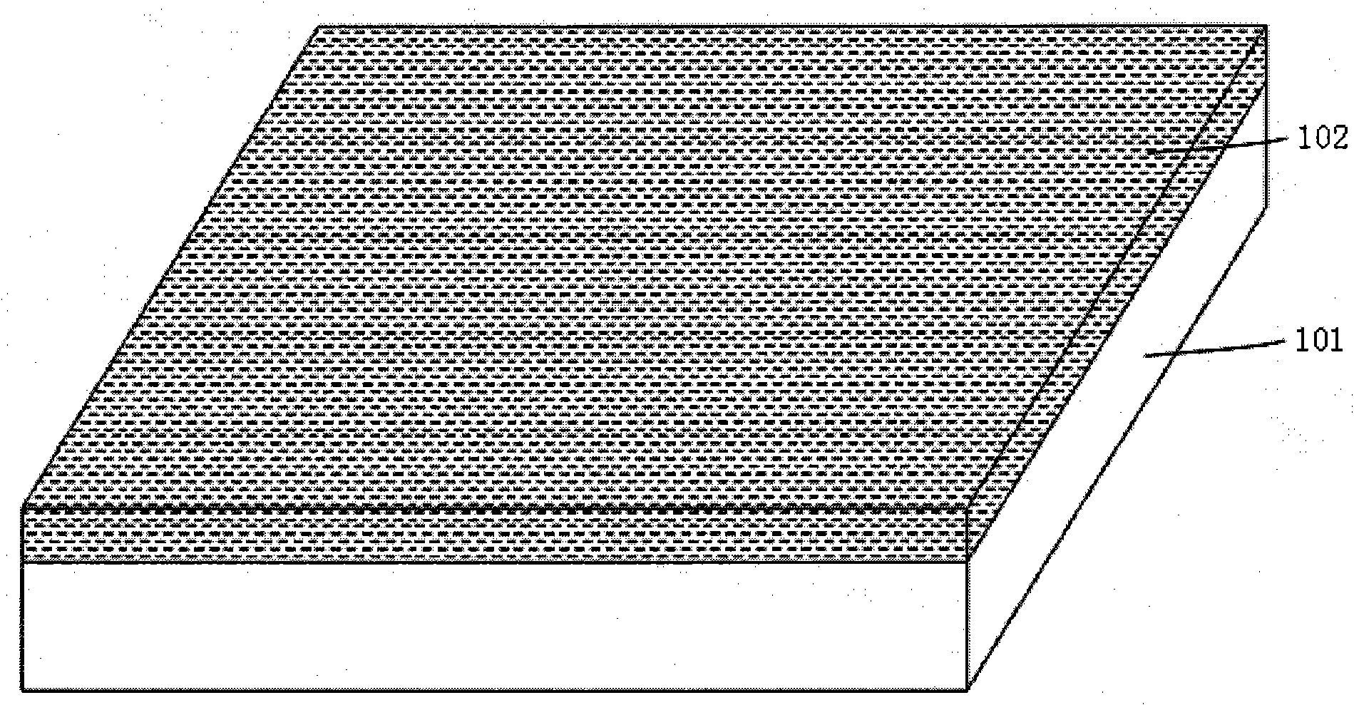
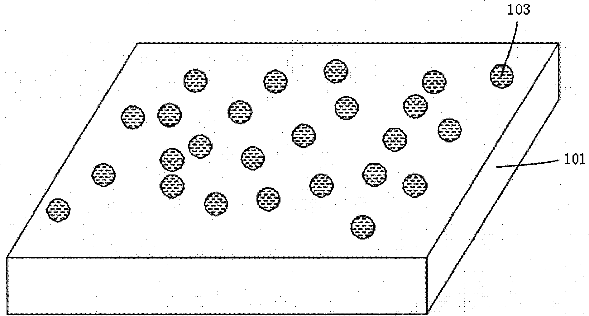
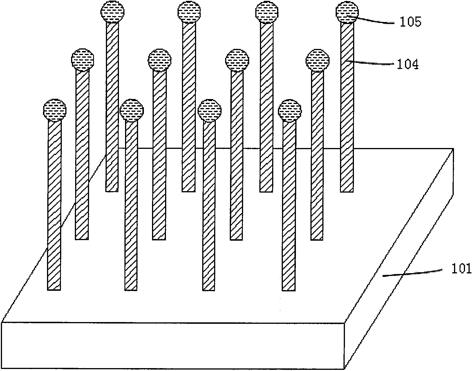
[0022] An exemplary embodiment of the present invention will be described in detail below with reference to the accompanying drawings. In the drawings, the thicknesses of layers and regions are enlarged or reduced for convenience of description, and the shown sizes do not represent actual sizes. Although these figures do not fully reflect the actual size of the device, they still completely reflect the mutual positions between the regions and the constituent structures, especially the upper-lower and adjacent relationships between the constituent structures. The referenced figures are schematic illustrations of idealized embodiments of the invention, and the illustrated embodiments of the invention should not be construed as limited to the particular shapes of regions illustrated in the figures but are to include resulting shapes, such as manufacturing-induced deviations. For example, the curves obtained by etching are usually curved or rounded, but in the embodiment of the prese
PUM
 Abstract
Description
Claims
Application Information
 - R&D Engineer
- R&D Manager
- IP Professional
- Industry Leading Data Capabilities
- Powerful AI technology
- Patent DNA Extraction
Browse by: Latest US Patents, China's latest patents, Technical Efficacy Thesaurus, Application Domain, Technology Topic.
© 2024 PatSnap. All rights reserved.Legal|Privacy policy|Modern Slavery Act Transparency Statement|Sitemap