Method of forming a backside electrode for use in a thin film solar cell
A technology of solar cells and back electrodes, applied in circuits, photovoltaic power generation, electrical components, etc., can solve the problems of waste of metal ingots, high operating costs, and cycle (long ineffective time), and achieve high-efficiency manufacturing and low-cost effects.
- Summary
- Abstract
- Description
- Claims
- Application Information
AI Technical Summary
Problems solved by technology
Method used
Image

Examples
Example Embodiment
[0077] Example 1
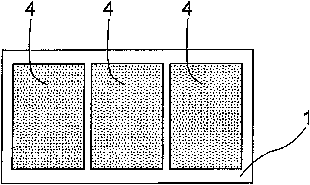
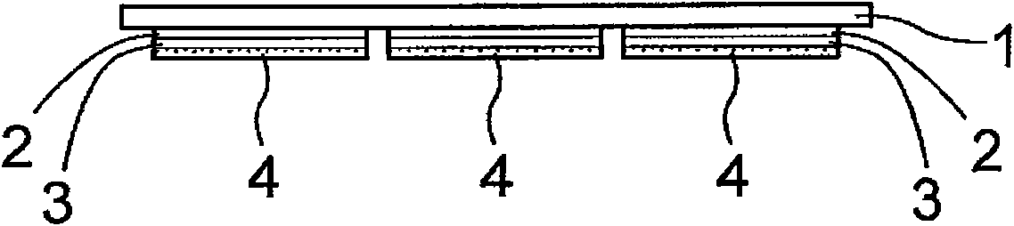
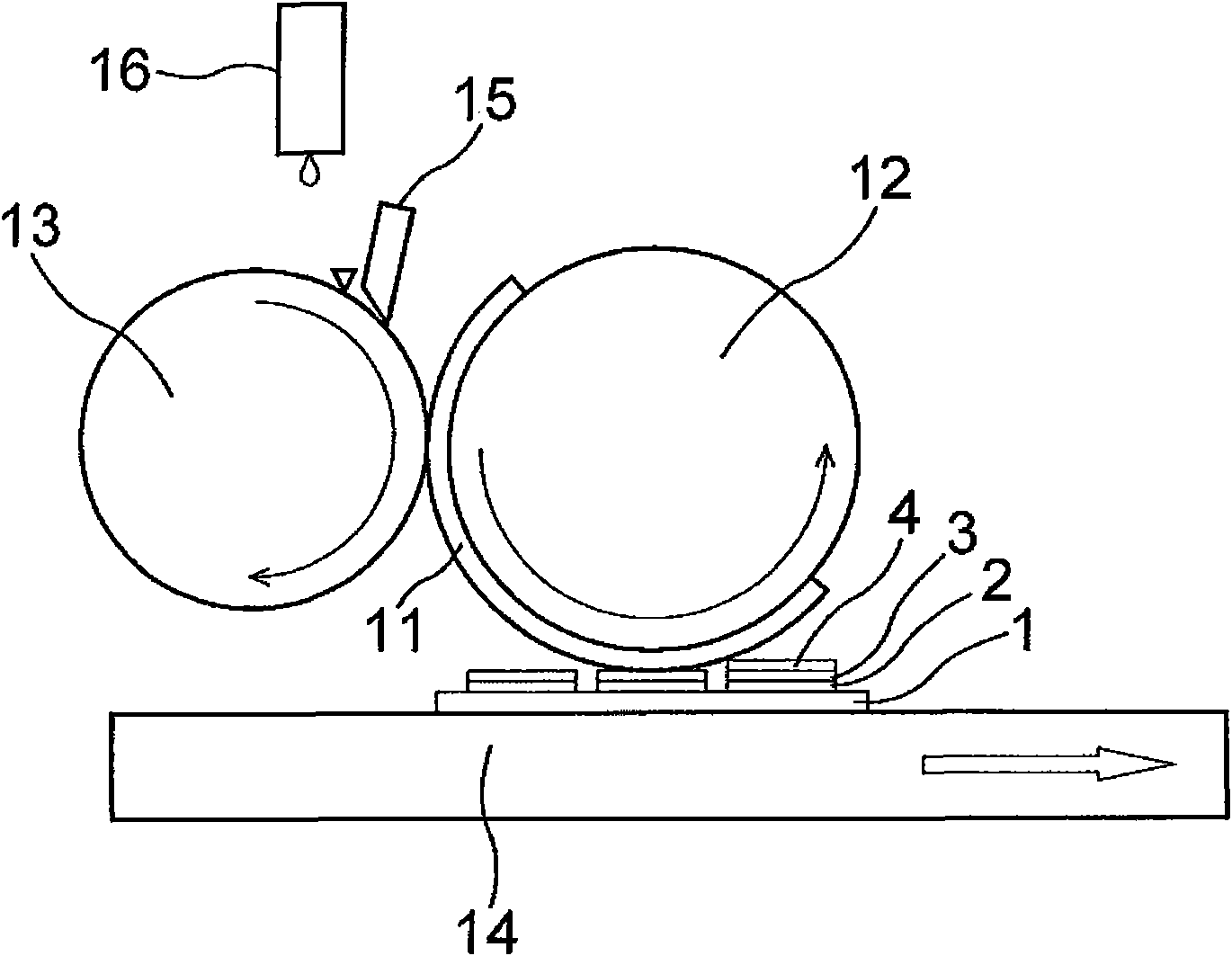
[0078] Under the above processing conditions, use a flexographic printing machine to print and transfer the nano silver conductive ink to the back of the substrate 1 on which the transparent electrode layer 2 and the photoelectric conversion layer 3 are pre-formed on the glass substrate. The temperature is 80°C for 5 minutes. After pre-baking it under the conditions, it is sintered (the temperature is increased from 70°C to 300°C within 30 minutes) to obtain a back electrode for thin-film solar cells with a film thickness of 0.4 μm.
PUM
| Property | Measurement | Unit |
|---|---|---|
| The average particle size | aaaaa | aaaaa |
| Viscosity | aaaaa | aaaaa |
| Film thickness | aaaaa | aaaaa |
Abstract
Description
Claims
Application Information
 - R&D Engineer
- R&D Manager
- IP Professional
- Industry Leading Data Capabilities
- Powerful AI technology
- Patent DNA Extraction
Browse by: Latest US Patents, China's latest patents, Technical Efficacy Thesaurus, Application Domain, Technology Topic.
© 2024 PatSnap. All rights reserved.Legal|Privacy policy|Modern Slavery Act Transparency Statement|Sitemap