Crucible and substrate slice for growing and casting monocrystalline silicon
A monocrystalline silicon and crucible technology, which is applied in the field of semiconductor crystalline silicon manufacturing, can solve the problems of large consumption of monocrystalline silicon blocks and high production costs, and achieve the effects of reducing consumption, reducing production costs and simplifying the operation process
- Summary
- Abstract
- Description
- Claims
- Application Information
AI Technical Summary
Benefits of technology
Problems solved by technology
Method used
Image

Examples
Embodiment 1
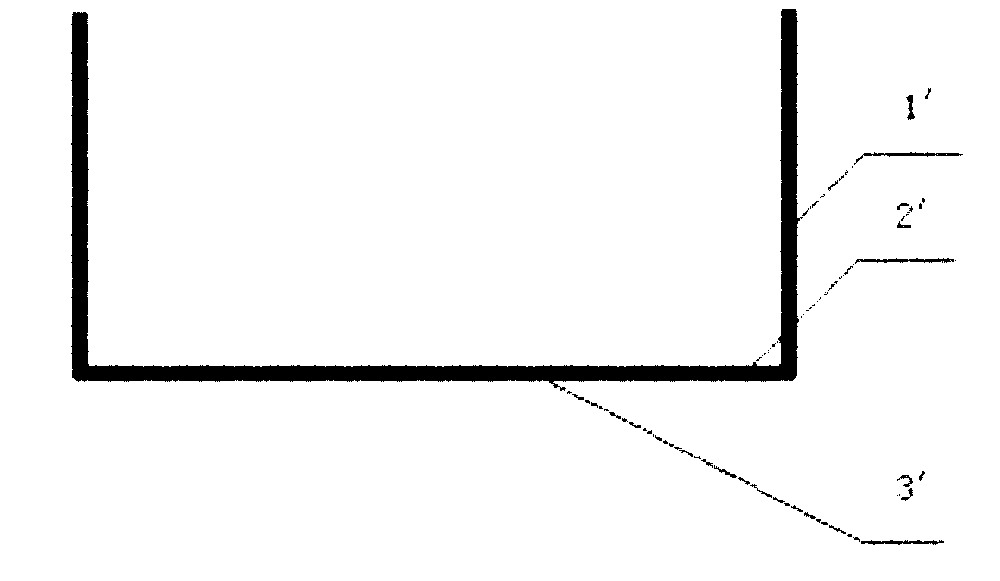
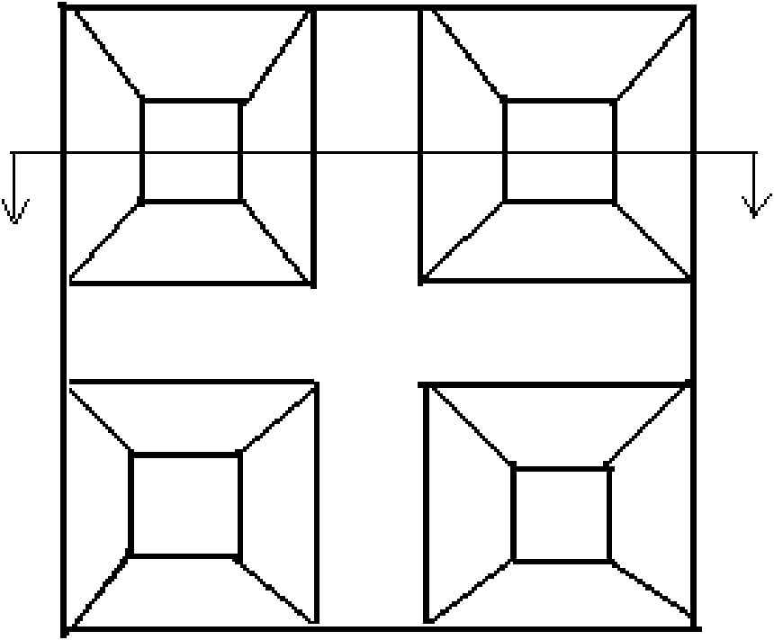
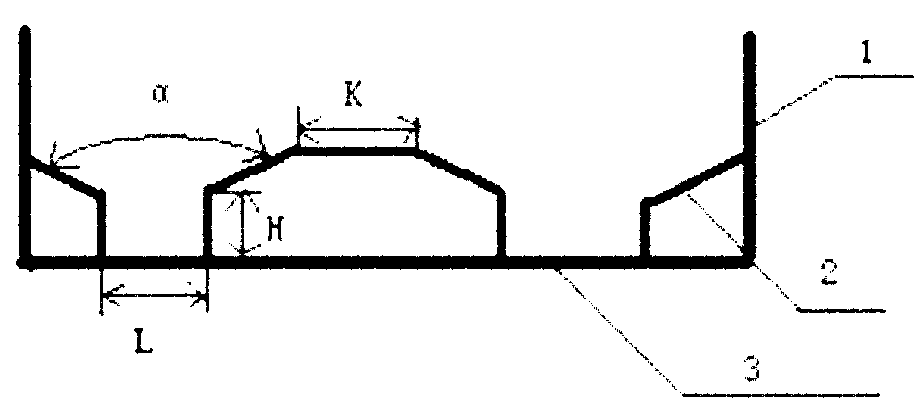
[0035] Such as image 3 In the crucible 1 shown, the inner wall 2 at the bottom of the crucible 1 is configured as several continuous crown-shaped structures, and the outer wall 3 at the bottom of the crucible 1 is a square structure. The top view of several continuous bucket crown structures is as follows figure 2 As shown, wherein, the cone angle α of each bucket crown structure is 90°-150°, the bottom dimension L is 0-10cm, the bottom height H is 0-10cm, and the distance K between adjacent bucket crown structures is 0-10cm. 10cm.
[0036] Such as image 3 When growing cast monocrystalline silicon in the crucible 1 shown, it is only necessary to place a small amount of monocrystalline silicon block as a seed crystal in the gap at the bottom of the crucible, then add polycrystalline silicon raw material and doping elements, and heat to completely melt the polycrystalline silicon raw material and doping elements 1. The monocrystalline silicon block is partially melted, and th
Embodiment 2
[0038] Such as Figure 7 In the crucible 1 shown, the inner wall 2 at the bottom of the crucible 1 is configured as several continuous cell structures, and the outer wall 3 at the bottom of the crucible 1 is a square structure. The top view of several continuous cell structures is as follows Figure 6 As shown, wherein, the bottom dimension L of each cell-shaped structure is 0-10 cm, the bottom height H is 0-10 cm, and the distance K between adjacent cell-shaped structures is 0-10 cm.
[0039] Such as Figure 7 When growing cast monocrystalline silicon in the crucible 1 shown, it is only necessary to place a small amount of monocrystalline silicon block as a seed crystal in the gap at the bottom of the crucible, then add polycrystalline silicon raw material and doping elements, and heat to completely melt the polycrystalline silicon raw material and doping elements 1. The monocrystalline silicon block is partially melted, and the insulation cover is lifted or cooling water is p
Embodiment 3
[0041] Such as Figure 11 In the crucible 1 shown, the inner wall 2 of the bottom of the crucible 1 is configured as several continuous hemispherical structures, and the outer wall 3 of the bottom of the crucible 1 is a square structure. The top view of several continuous hemispherical structures is as follows Figure 10 As shown, wherein, the bottom dimension L of each hemispherical structure is 0-10cm, and the bottom height H is 0-10cm.
[0042] use as Figure 11 In the shown crucible 1, only a small amount of monocrystalline silicon block needs to be placed in the gap at the bottom of the crucible as a seed crystal, and then polycrystalline silicon raw material and doping elements are put in, heated to completely melt the polycrystalline silicon raw material and doping element, and the monocrystalline silicon block Partially melt, lift the insulation cover or pass cooling water at the bottom of the crucible for heat exchange, and the single crystal silicon block acts as a se
PUM
| Property | Measurement | Unit |
|---|---|---|
| Cone angle | aaaaa | aaaaa |
| Size | aaaaa | aaaaa |
| Height | aaaaa | aaaaa |
Abstract
Description
Claims
Application Information
 - R&D Engineer
- R&D Manager
- IP Professional
- Industry Leading Data Capabilities
- Powerful AI technology
- Patent DNA Extraction
Browse by: Latest US Patents, China's latest patents, Technical Efficacy Thesaurus, Application Domain, Technology Topic.
© 2024 PatSnap. All rights reserved.Legal|Privacy policy|Modern Slavery Act Transparency Statement|Sitemap