Switching noise suppression circuit integrated on A/D (analog/digital) converter chip
A technology for switching noise and suppressing circuits, applied in the field of switching noise suppressing circuits, can solve problems such as performance degradation of A/D converters, and achieve the effects of improving dynamic performance and improving compatibility
- Summary
- Abstract
- Description
- Claims
- Application Information
AI Technical Summary
Benefits of technology
Problems solved by technology
Method used
Image

Examples
Embodiment Construction
[0024] The specific implementation manners of the present invention are not limited to the following description, and are now further described in conjunction with the accompanying drawings.
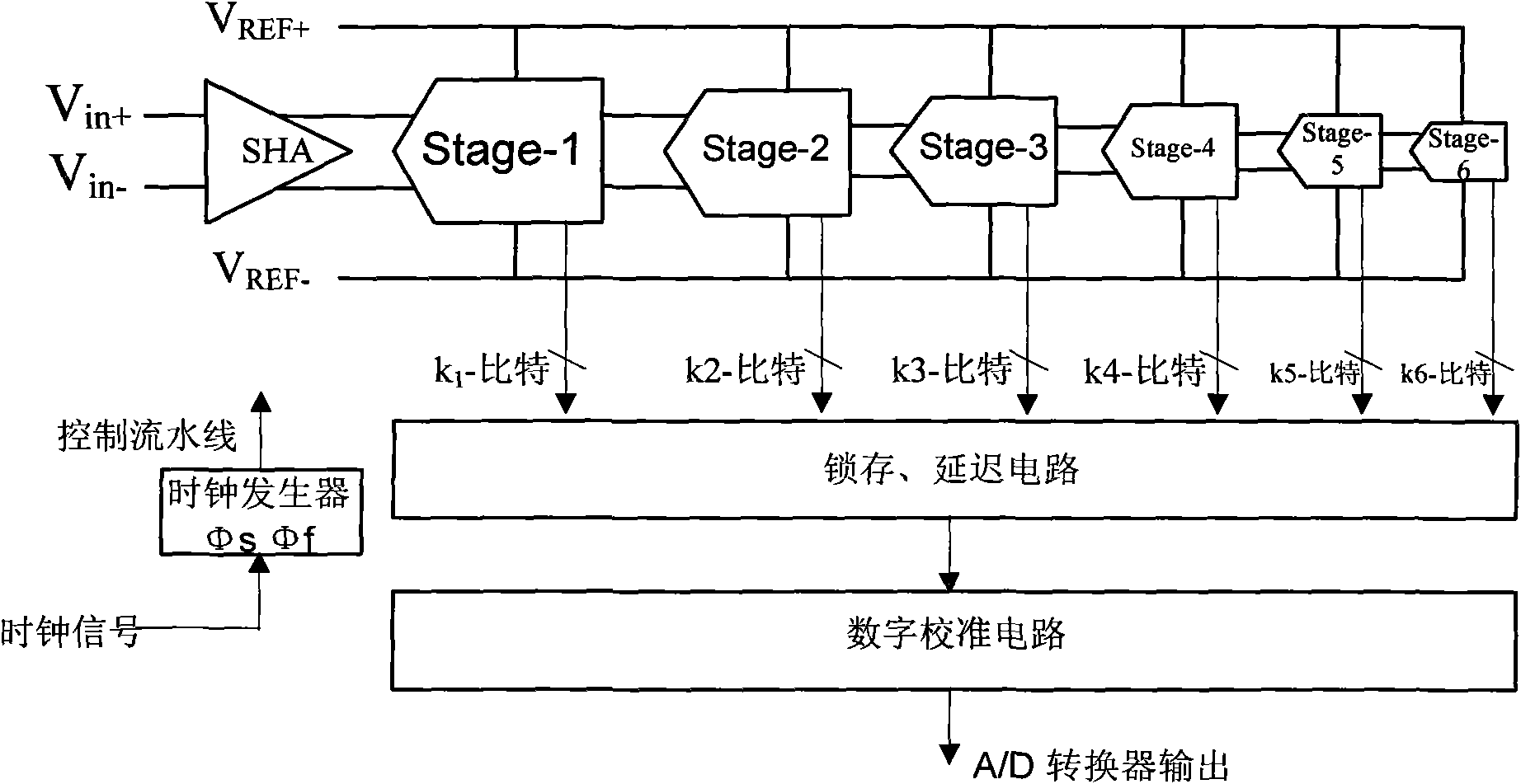
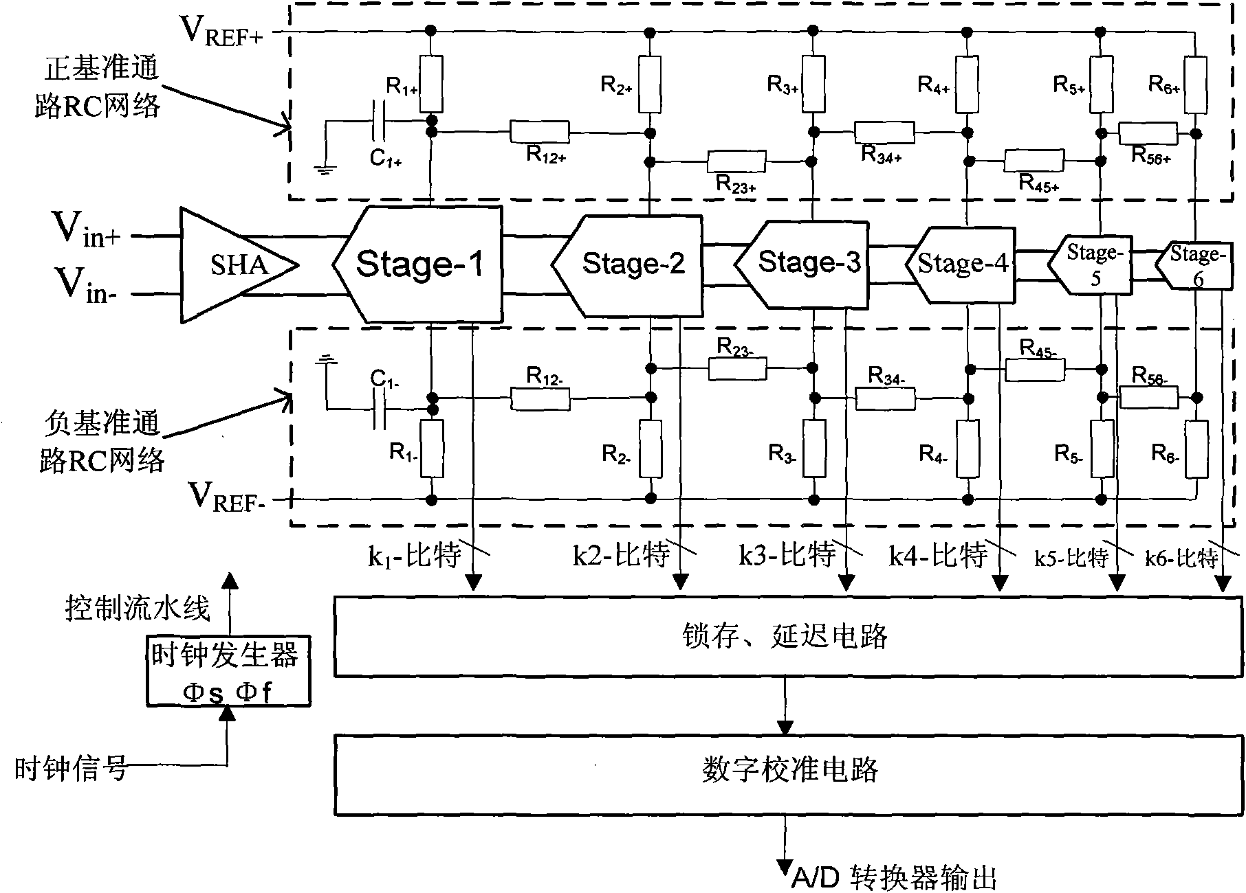
[0025] The circuit diagram of the switching noise suppression circuit integrated on the A / D converter chip implemented by the present invention is as figure 2 shown. It consists of a positive reference pass RC network and a negative reference pass RC network.
[0026] figure 2 The specific connection relationship and functional relationship in are the same as the content of the invention in this specification, and will not be repeated here. It works like this:
[0027] Using the SSN peak model proposed by Yungseon Eo et al.:
[0028] V n max ≈ n L p β n 2
PUM
 Abstract
Description
Claims
Application Information
 - R&D Engineer
- R&D Manager
- IP Professional
- Industry Leading Data Capabilities
- Powerful AI technology
- Patent DNA Extraction
Browse by: Latest US Patents, China's latest patents, Technical Efficacy Thesaurus, Application Domain, Technology Topic.
© 2024 PatSnap. All rights reserved.Legal|Privacy policy|Modern Slavery Act Transparency Statement|Sitemap