Semiconductor device

A semiconductor and metal technology, applied in the field of semiconductor devices, can solve problems such as short circuit of modules, and achieve the effect of improving heat dissipation and improving product qualification rate

Inactive Publication Date: 2011-12-21
PANASONIC CORP
View PDF8 Cites 2 Cited by
  • Summary
  • Abstract
  • Description
  • Claims
  • Application Information

AI Technical Summary

Benefits of technology

The technical effect described by this patented technology relates to improving the performance and efficiency of electronic devices that use metals for their components while also reducing temperature during operation. By arranging certain parts nearer the central region where the device's active elements are located, these materials help absorb more energy than other areas on the circuit board or directly onto them. This helps prevent overheated chips caused by excessive power usage without affecting any nearby circuits.

Problems solved by technology

Technological Problem addressed by these two technical documents relating to improving the performance of leadless chip carriages with improved heat dissipation efficiency during operation under severe conditions such as temperatures approaching 350 degrees Celsium.

Method used


Image

  • Semiconductor device
  • Semiconductor device
  • Semiconductor device

Examples


Embodiment Construction

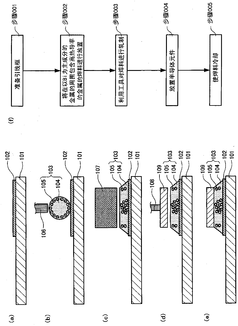
[0020] Hereinafter, embodiments of the present invention will be described in detail with reference to the drawings. In this embodiment, a description will be given of a semiconductor device in which a semiconductor element and a support plate are bonded by solder containing Bi as a main component.

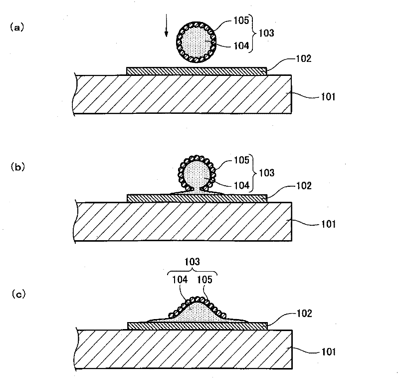
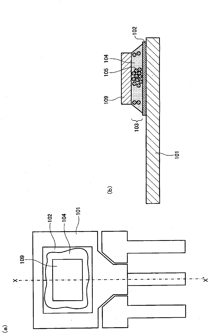
[0021] First, the manufacturing process of the semiconductor device according to this embodiment will be described. figure 1 (a)~ figure 1 (f) is a flowchart showing the manufacturing process of the semiconductor device according to this embodiment. in particular, figure 1 (a)~ figure 1 (e) shows a schematic cross-sectional view of each manufacturing process, figure 1 (f) shows the flowchart shown by step 001 - step 005 corresponding to each manufacturing process. This manufacturing process is a process for manufacturing a semiconductor device having a die bond junction excellent in thermal conductivity.

[0022] First, use figure 1 (a) Step 001 is described. In step 001, a l


PUM

PropertyMeasurementUnit
Thermal conductivityaaaaaaaaaa
Melting pointaaaaaaaaaa

Abstract

A semiconductor device of the present invention includes a supporting board, an electrode surface processing layer formed on the supporting board, a semiconductor element, and a solder material containing a first metal composed mainly of bismuth and a second metal having a higher melting point than the first metal and joining the electrode surface processing layer and the semiconductor element, the first metal containing particles of the second metal inside the first metal. The composition ratio of the second metal is higher than the first metal in a region of the solder material corresponding to the center portion of the semiconductor element, and the composition ratio of the second metal is at least 83.8 atomic percent in the region corresponding to the center portion.

Description


Claims


Application Information

Patent Timeline
Owner PANASONIC CORP
Why Eureka
Try Eureka