Method for preparing double-stress thin film

A dual-stress, thin-film technology, which is applied in semiconductor/solid-state device manufacturing, electrical components, circuits, etc., can solve the problems of plasma damage, increase the difficulty of process control, and the device speed cannot meet the process requirements, so as to solve the loss of yield rate , to avoid the effect of overlapping area problems

Inactive Publication Date: 2012-08-15
SHANGHAI HUALI MICROELECTRONICS CORP
View PDF6 Cites 8 Cited by
  • Summary
  • Abstract
  • Description
  • Claims
  • Application Information

AI Technical Summary

Problems solved by technology

[0003]However, at present, the industry generally chooses silicon nitride film as the double stress film. Since the dielectric constant of silicon nitride film is relatively high (k is generally around 7.0), it will It causes a certain time delay (RC delay), that is, it cannot meet the requirements of some advanced devices for time delay (RC delay), and the speed of the device cannot meet the process requirements.
[0004]In the current integration process, for the problem of overlap of different stress films, it is mainly adjusted by using dry etching process or considered in layout design to try to Reduce the impact on yield, but increase the difficulty of process control
[0005]Figure 1 is a schematic diagram of the flow structu

Method used


Image

  • Method for preparing double-stress thin film
  • Method for preparing double-stress thin film
  • Method for preparing double-stress thin film

Examples


Embodiment Construction

[0018] The specific embodiment of the present invention will be further described below in conjunction with accompanying drawing:

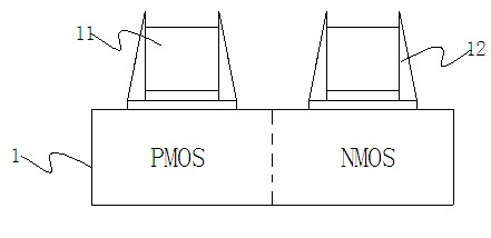
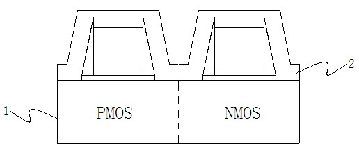
[0019] Figure 2-8 It is a schematic structural diagram of the technological process of the preparation method of a double stress thin film of the present invention.

[0020] like Figure 2-8 As shown, first, nitrogen-doped silicon carbide (Nitrogen Doped Carbide, NDC for short) 2 is deposited on the PMOS and NMOS structures 1 including the gate 11 and sidewalls 12, and the nitrogen-doped silicon carbide film 2 covers the gate 11 and sidewalls 12; after that, spin-coat photoresist to cover the upper surface of the nitrogen-doped silicon carbide film 2, remove the remaining photoresist after exposure and development, and form the first photoresist 3 covering the PMOS structure.

[0021] Then, using the first light source 3 as a mask, an ultraviolet (UV) light irradiation process 4 is performed on the nitrogen-doped carbide film 2, so that the nitrog


PUM


Abstract

The invention relates to the field of semiconductor manufacture, in particular to a method for preparing a double-stress thin film. The method for preparing the double-stress thin film is used for preparing a high-stress double-stress thin film by replacing a traditional silicon nitride thin film with a nitride-doped silicon carbide thin film. The method for preparing the double-stress thin film can not only meet the requirements of RC (resistance capacitance) delay of a plurality of advanced devices, but also avoid the problem of existence of an overlapping area in the traditional silicon nitride double-stress thin film process, thereby solving the loss of yield caused by the overlapping area; and the method for preparing the double-stress thin film is simple and easy to implement.

Description


Claims


Application Information

Patent Timeline
Owner SHANGHAI HUALI MICROELECTRONICS CORP
Why Eureka
Try Eureka