Method for manufacturing stable high temperature-resistant hydrogen end group conducting channel on diamond surface
A surface fabrication and conductive channel technology, which is applied in the manufacture of circuits, electrical components, semiconductors/solid-state devices, etc., can solve the problems of p-type channel failure, adsorption layer and hydrogen end group decomposition, and large environmental impact, and achieve the realization of normal working effect
- Summary
- Abstract
- Description
- Claims
- Application Information
AI Technical Summary
Problems solved by technology
Method used
Image

Examples
Embodiment 1
[0025] Example 1: (1) A high-resistance diamond of 300 μm was grown on a molybdenum substrate by microwave plasma chemical vapor deposition;
[0026] (2) Form a p-type conductive channel on the high-resistance diamond material by hydrogen plasma treatment for 30 minutes;
[0027] (3) The hydrogen-terminated diamond obtained after treatment is placed in a chemical vapor deposition equipment and vacuumed to 10 -4 mbar, then into NH 3 and H 2 The mixture of which NH 3 The flow rate is 500mL / min, H 2 The flow rate is 20L / min, the reaction chamber pressure is 100mbar, and the treatment time is 1 hour.
[0028] (4) After taking out the sample, deposit 3nm HfO in the atomic layer deposition equipment at room temperature 2 The dielectric barrier layer prevents the surface of the hydrogen-terminated diamond adsorbed with polar molecules and functional groups from being directly exposed to the environment.
Embodiment 2
[0029] Example 2: (1) A high-resistance diamond of 300 μm was grown on a molybdenum substrate by a direct current arc method;
[0030] (2) Form a p-type conductive channel on the high-resistance diamond material by hydrogen plasma treatment for 30 minutes;
[0031] (3) Soak the hydrogen-terminated diamond obtained after treatment in trimellitic anhydride TMA for 30 min;
[0032] (4) After taking out the sample, deposit 3nm Al in the atomic layer deposition equipment at room temperature 2 o 3 The dielectric barrier layer prevents the surface of the hydrogen-terminated diamond adsorbed with polar molecules and functional groups from being directly exposed to the environment.
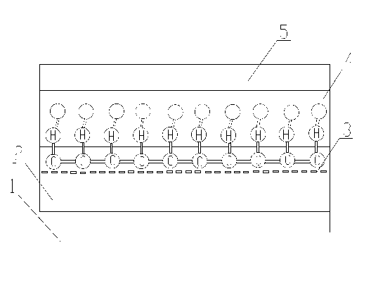
[0033] When this hydrogen-terminated diamond is exposed to an atmosphere of polar molecules, it will adsorb the polar molecules and form an electrochemical system. In this system, the electronegativity of the C-H dipole is 1.3eV, and the valence band is higher than The chemical potential of adsorbed polar
PUM
 Abstract
Description
Claims
Application Information
 - R&D Engineer
- R&D Manager
- IP Professional
- Industry Leading Data Capabilities
- Powerful AI technology
- Patent DNA Extraction
Browse by: Latest US Patents, China's latest patents, Technical Efficacy Thesaurus, Application Domain, Technology Topic.
© 2024 PatSnap. All rights reserved.Legal|Privacy policy|Modern Slavery Act Transparency Statement|Sitemap