Manufacturing method for low-temperature polycrystalline silicon thin film transistor and array substrate

A low-temperature polysilicon, thin film transistor technology, applied in semiconductor/solid-state device manufacturing, semiconductor devices, electrical components, etc., can solve problems such as poor contact of the active layer

Active Publication Date: 2014-09-03
BOE TECH GRP CO LTD
View PDF8 Cites 1 Cited by
  • Summary
  • Abstract
  • Description
  • Claims
  • Application Information

AI Technical Summary

Problems solved by technology

[0005] The technical problem to be solved by the present invention is to provide a method for manufacturing a low-temperature polysilicon thin film trans...

Method used


Image

  • Manufacturing method for low-temperature polycrystalline silicon thin film transistor and array substrate
  • Manufacturing method for low-temperature polycrystalline silicon thin film transistor and array substrate
  • Manufacturing method for low-temperature polycrystalline silicon thin film transistor and array substrate

Examples


Embodiment Construction

[0044] The following will clearly and completely describe the technical solutions in the embodiments of the present invention with reference to the accompanying drawings in the embodiments of the present invention. Obviously, the described embodiments are some of the embodiments of the present invention, but not all of them. Based on the embodiments of the present invention, all other embodiments obtained by persons of ordinary skill in the art without making creative efforts belong to the protection scope of the present invention.

[0045] Embodiments of the present invention provide a method for manufacturing a low-temperature polysilicon thin film transistor and a method for manufacturing an array substrate, which can solve the technical problem of poor contact between a source or a drain and an active layer.

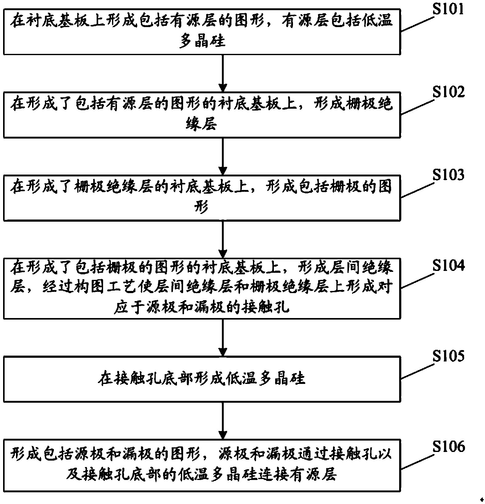
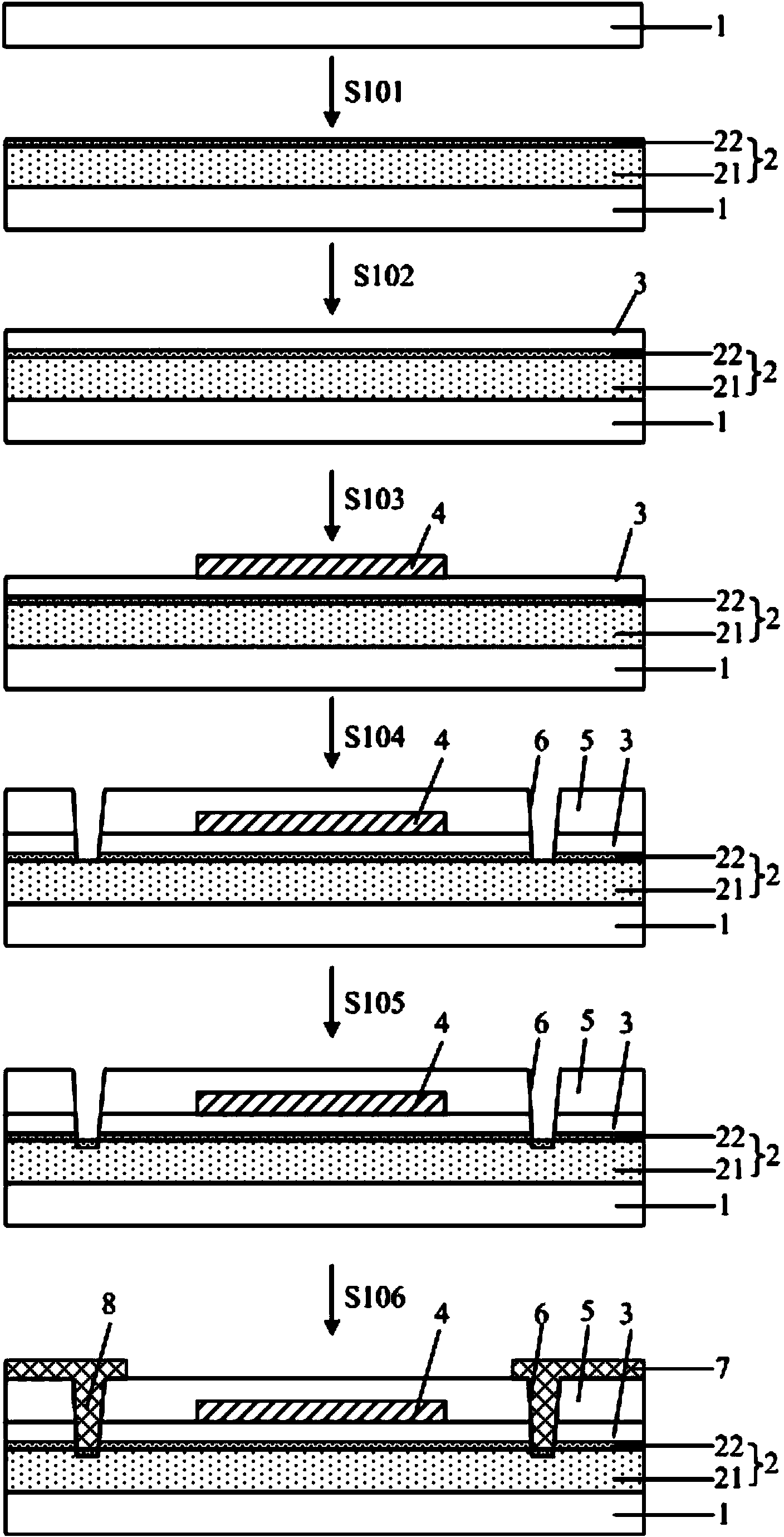
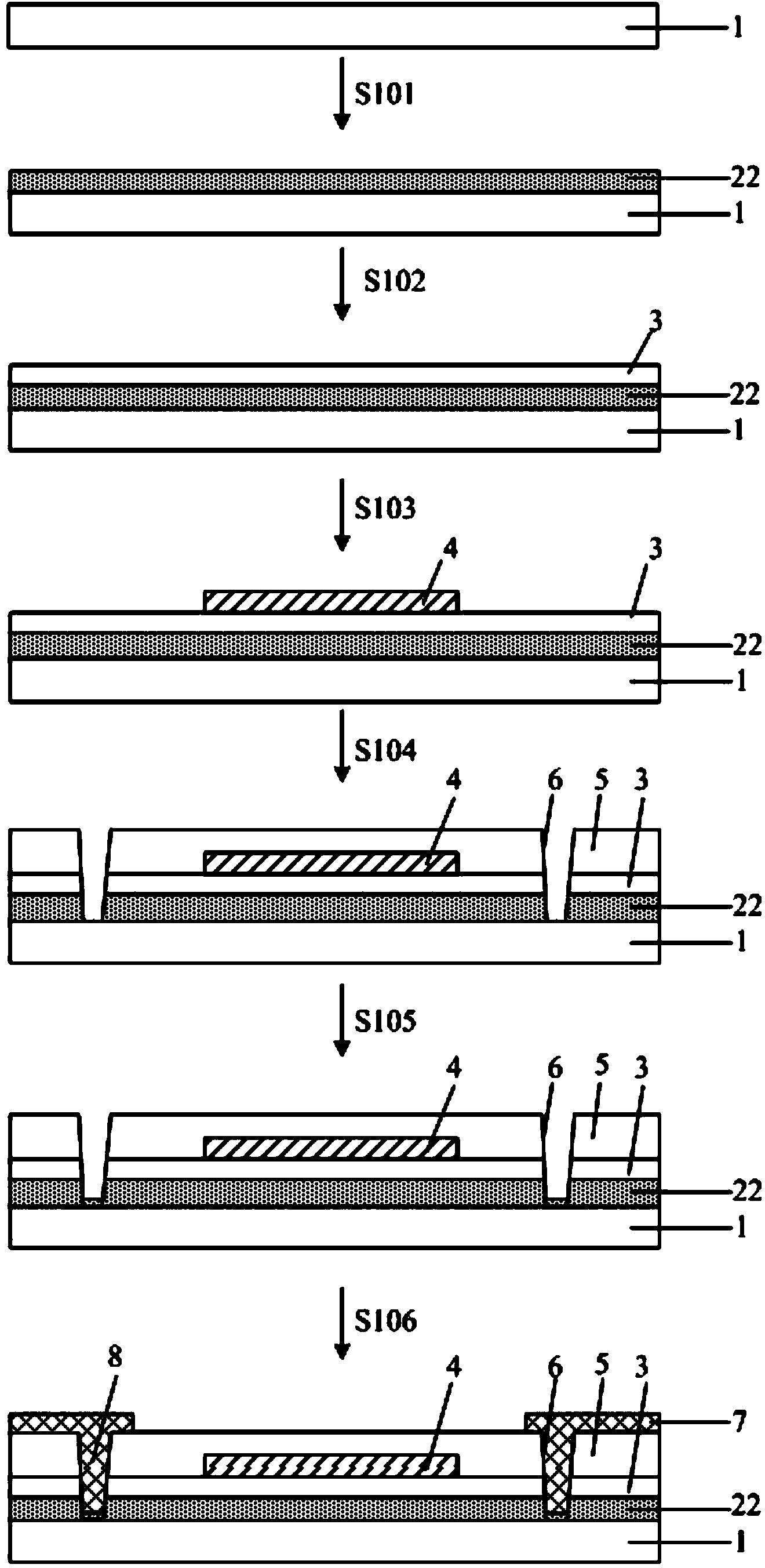
[0046] Specifically, such as figure 1 As shown, the manufacturing method of the low temperature polysilicon thin film transistor comprises the following steps:

[0...


PUM


Abstract

The embodiment of the invention discloses a manufacturing method for a low-temperature polycrystalline silicon thin film transistor and an array substrate and relates to the technical field of display. The manufacturing method solves the technical problem that a source electrode or a drain electrode does not make good contact with an active layer. The manufacturing method comprises the steps that a pattern containing the active layer is formed on a substrate, wherein the active layer contains low-temperature polycrystalline silicon; a gate insulation layer is formed on the substrate where the pattern containing the active layer is formed; a pattern containing a grid electrode is formed on the substrate where the gate insulation layer is formed; an interlayer insulating layer is formed on the substrate where the pattern containing the grid electrode is formed, and contact holes corresponding to the source electrode and the drain electrode are formed in the interlayer insulating layer and the gate insulation layer through a composition process; the low-temperature polycrystalline silicon is formed at the bottoms of the contact holes; a pattern containing the source electrode and the drain electrode is formed, and the source electrode and the drain electrode are connected with the active layer through the contact holes and the low-temperature polycrystalline silicon at the bottoms of the contact holes.

Description

technical field [0001] The invention relates to the field of display technology, in particular to a method for manufacturing a low-temperature polysilicon thin film transistor and a method for manufacturing an array substrate. Background technique [0002] Due to the advantages of low-temperature polysilicon thin-film transistors such as high electron mobility, fast response speed, and good stability, currently, commonly used active-matrix liquid crystal displays mostly use low-temperature polysilicon thin-film transistors. [0003] Specifically, the manufacturing method of the low-temperature polysilicon thin film transistor is as follows: first, a layer of amorphous silicon is formed on the substrate; secondly, the upper layer of the amorphous silicon is converted into low-temperature polysilicon by an excimer laser annealing process to form an active transistor. layer; again, sequentially form a gate insulating layer, a gate and an interlayer insulating layer; then, etch ...

Claims


Application Information

Patent Timeline
Patent Type & Authority Applications(China)
IPC IPC(8): H01L21/336H01L21/78
CPCH01L21/76882H01L21/76895H01L29/66757H01L2021/775
Inventor 李良坚左岳平
Owner BOE TECH GRP CO LTD
Why Eureka
Try Eureka