Thin film solar cell production method and electrodeposition device thereof
A technology for solar cells and electrodeposition devices, applied in circuits, photovoltaic power generation, electrical components, etc., can solve the problems of reducing the effective area and affecting the conversion efficiency of light absorption, so as to reduce the contact resistance, improve the electrodeposition efficiency, and increase the contact area effect
- Summary
- Abstract
- Description
- Claims
- Application Information
AI Technical Summary
Problems solved by technology
Method used
Image

Examples
Example Embodiment
[0075] Example 1
[0076] Figure 1a-2p The method for producing the thin-film solar cell 1 in this embodiment is shown, including the following steps:
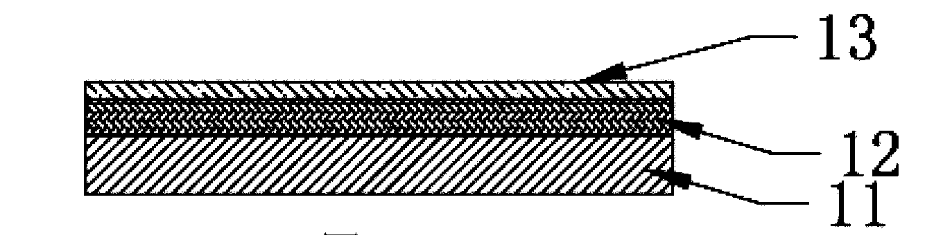
[0077] (A) Depositing a transparent conductive layer 12 (Transparent conductive oxide, TCO for short) on the glass substrate 11;
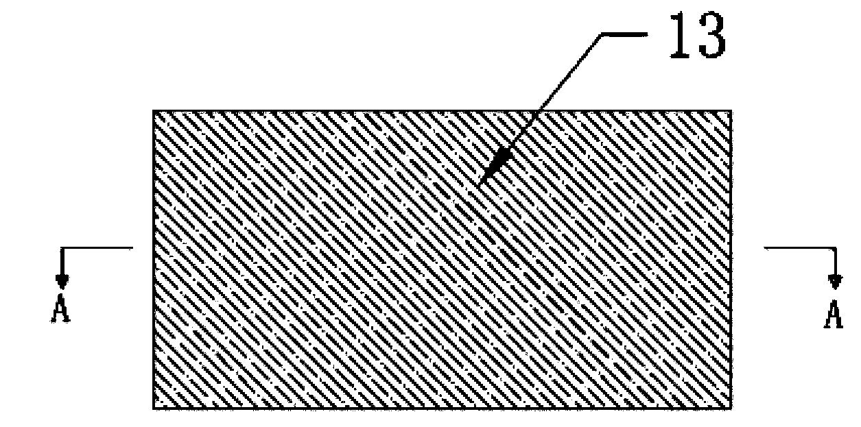
[0078] (B) A window layer 13 is formed on the transparent conductive layer 12. In this embodiment, the window layer 13 is cadmium sulfide (CdS), and the window layer 13 is formed on the transparent conductive layer 12 by electrodeposition;
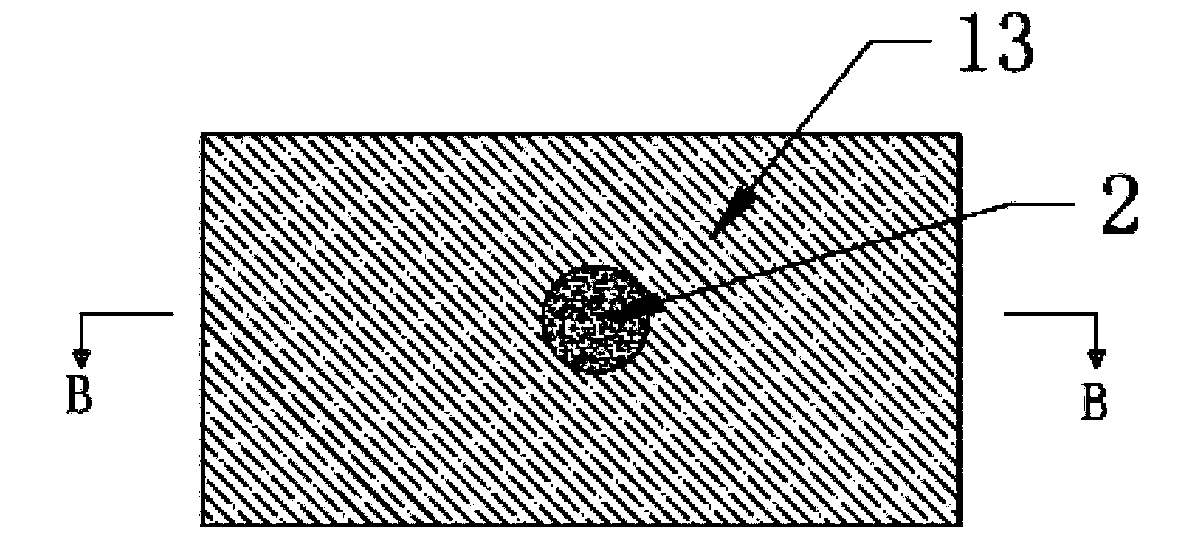
[0079] (C) The contact electrode 2 penetrates the window layer 13 to make ohmic contact with the transparent conductive layer 12, and the above-mentioned semi-finished product is placed in the electrodeposition tank, and the contact electrode 2 and the counter electrode are energized, in the window layer 13. Electrodeposit an absorption layer 14 on the electrode. The absorption layer 14 is cadmium telluride (CdTe). In this embodiment, the cross section of the contact ele
Example Embodiment
[0092] Example 2
[0093] Figure 3a-3p Shown in this embodiment is a method for producing a thin-film solar cell 1 which includes the following steps:
[0094] (A) Depositing a transparent conductive layer 12 (Transparent conductive oxide, TCO for short) on the glass substrate 11;
[0095] (B) A window layer 13 is formed on the transparent conductive layer 12. In this embodiment, the window layer 13 is cadmium sulfide (CdS);
[0096] (C) The contact electrode 2 penetrates the window layer 13 to make ohmic contact with the transparent conductive layer 12, and the above-mentioned semi-finished product is placed in the electrodeposition tank, and the contact electrode 2 and the counter electrode are energized. 13. The absorption layer 14 is electrodeposited. In this embodiment, the cross section of the contact electrode 2 parallel to the glass substrate 11 is rectangular;
[0097] (D) Remove the contact electrode 2 and create a contact electrode vacancy 15 at the original contact electrode
PUM
 Abstract
Description
Claims
Application Information
 - R&D Engineer
- R&D Manager
- IP Professional
- Industry Leading Data Capabilities
- Powerful AI technology
- Patent DNA Extraction
Browse by: Latest US Patents, China's latest patents, Technical Efficacy Thesaurus, Application Domain, Technology Topic.
© 2024 PatSnap. All rights reserved.Legal|Privacy policy|Modern Slavery Act Transparency Statement|Sitemap