Plasma processing chamber and base manufacturing method therefor
A manufacturing method, plasma technology, applied in the manufacture of ships or leading wires, etc., to achieve the effect of preventing arc discharge and metal pollution
- Summary
- Abstract
- Description
- Claims
- Application Information
AI Technical Summary
Benefits of technology
Problems solved by technology
Method used
Image

Examples
Embodiment Construction
[0022] The specific embodiments of the present invention will be described below in conjunction with the accompanying drawings.
[0023] It should be pointed out that the words "semiconductor process piece", "wafer" and "substrate" will often be used interchangeably in the following description, and in the present invention, they all refer to the process processed in the processing chamber. The process parts are not limited to wafers, substrates, substrates, large-area flat substrates, etc. For the convenience of description, the "substrate" will be used as an example in the description and illustrations of the embodiments herein.
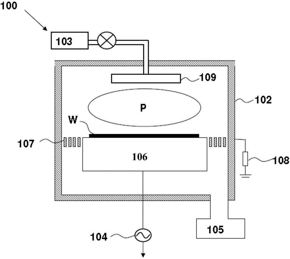
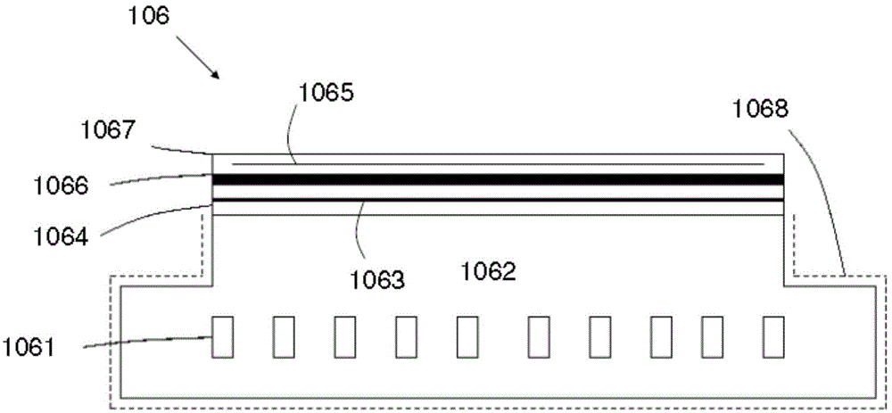
[0024] figure 1 A schematic structural view of a plasma processing chamber is shown. The plasma processing chamber 100 has a processing chamber (not shown), the processing chamber is substantially cylindrical, and the side wall 102 of the processing chamber is substantially vertical, and there are upper electrodes and lower electrodes arranged paral
PUM
 Abstract
Description
Claims
Application Information
 - R&D Engineer
- R&D Manager
- IP Professional
- Industry Leading Data Capabilities
- Powerful AI technology
- Patent DNA Extraction
Browse by: Latest US Patents, China's latest patents, Technical Efficacy Thesaurus, Application Domain, Technology Topic.
© 2024 PatSnap. All rights reserved.Legal|Privacy policy|Modern Slavery Act Transparency Statement|Sitemap